
Datasheet


Debug
Power
Domain
Target and
BoosterPack
Power
Domain
Legend
J101
3V3
eZ-FET
J1
J2
MSP430FR4133
target and
BoosterPack
VCC
GND
GND
J6
Target
MSP430FR4133
Device
LCD
USB (eZ-FET) Power
Configuration
Place
Jumper
BoosterPack and External
Power Configuration
J101
3V3
eZ-FET
J1
J2
MSP430FR4133
target and
BoosterPack
VCC
GND
GND
J6
Target
MSP430FR4133
Device
LCD
No
Jumper
Hardware
www.ti.com
14
SLAU595A–October 2014–Revised July 2015
Submit Documentation Feedback
Copyright © 2014–2015, Texas Instruments Incorporated
MSP430FR4133 LaunchPad™ Development Kit (MSP
‑
EXP430FR4133)
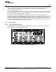
2.3 Power
The board was designed to accommodate various powering methods, including through the on-board eZ-
FET and from external or BoosterPack power (see Figure 9).
Figure 9. MSP-EXP430FR4133 Power Block Diagram
2.3.1 eZ-FET USB Power
The most common power-supply scenario is from USB through the eZ-FET debugger. This provides 5-V
power from the USB and also regulates this power rail to 3.3 V for eZ-FET operation and 3.3 V to the
target side of the LaunchPad. Power from the eZ-FET is controlled by jumper J101. For 3.3 V, make sure
that a jumper is connected across the J101 3V3 terminal.
2.3.2 BoosterPack and External Power Supply
Header J6 is present on the board to supply external power directly. It is important to comply with the
device voltage operation specifications when supplying external power. The MSP430FR4133 has an
operating range of 1.8 V to 3.6 V. More information can be found in the MSP430FR4133 data sheet
(SLAS865).