
Datasheet


#$
#$
#$$
SBAS317E − APRIL 2004 − REVISED MAY 2006
www.ti.com
19
DESCRIPTION
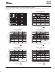
The MSC1200Yx, MSC1201Yx, and MSC1202Yx are
completely integrated families of mixed-signal devices
incorporating a high-resolution, delta-sigma ADC, 8-bit
cuurent output DAC, input multiplexer, burnout detect
current sources, selectable buffered input, offset DAC,
programmable gain amplifier (PGA), temperature sensor,
voltage reference, 8-bit 8051 microcontroller, Flash
Program Memory, Flash Data Memory, and Data SRAM,
as shown in Figure 3. The MSC1200, MSC1201, and
MSC1202 will be referred to as the MSC120x in this
document, unless otherwise noted.
On-chip peripherals include an additional 32-bit
summation register, basic SPI, basic I
2
C, USART, two
8-bit digital input/output ports, a watchdog timer,
low-voltage detect, on-chip power-on reset, brownout
reset, timer/counters, system clock divider, PLL, on-chip
oscillator, and external or internal interrupts.
The devices accept differential or single-ended signals
directly from a transducer. The ADC provides 24 bits
(MSC1200/01) or 16 bits (MSC1202) of resolution and 24
bits (MSC1200/01) or 16 bits (MSC1202) of
no-missing-code performance using a Sinc
3
filter with a
programmable sample rate. The ADC also has a
selectable filter that allows for high-resolution, single-cycle
conversions.
The microcontroller core is 8051 instruction set
compatible. The microcontroller core is an optimized 8051
core that executes up to three times faster than the
standard 8051 core, given the same clock source. This
design makes it possible to run the device at a lower
external clock frequency and achieve the same
performance at lower power than the standard 8051 core.
The MSC120x allow users to uniquely configure the Flash
Memory map to meet the needs of their applications. The
Flash is programmable down to +2.7V using serial
programming. Flash endurance is typically 1M
Erase/Write cycles.
The parts have separate analog and digital supplies, which
can be independently powered from +2.7V to +5.25V. At
+3V operation, the power dissipation for the part is
typically less than 3mW. The MSC1200 is available in a
TQFP-48 package. The MSC1201 and MSC1202 are both
available in a QFN-36 package.
The MSC120x are designed for high-resolution
measurement applications in smart transmitters, industrial
process control, weigh scales, chromatography, and
portable instrumentation.
MUX
AV
DD
BUF PGA
V
REF
Modulator
4K or 8K
FLASH
256 Bytes
SRAM
128 Bytes
System FLASH
Digital
Filter
32−Bit ACC
8051
SFR
ALVD
DBOR
POR
System
Clock
Divider
PORT1
WDT
Alternate
Functions
Timers/
Counters
PLL
PORT3
DIN
DOUT
SS
EXT (4)
PROG
USART0
EXT (2)
T0
T1
SCK/SCL/CLKS
On−Chip
Oscillator
8−Bit
Offset DAC
8−Bit IDAC
Burnout
Detect
AIN0
AIN1
AIN2
AIN3
AIN4
AIN5
AIN6
(2)
AIN7
(2)
AINCOM
IDAC
AGND REFOUT/REFIN+ DV
DD
DGND
XIN XOUT
Temperature
Sensor
Burnout
Detect
RST
AGND
AV
DD
REF IN
−
(1)
(1) REF IN
−
must be tied to AGND when using internal V
REF
.
(2) AIN6 and AIN7 available only on MSC1200.
NOTES:
Figure 3. Block Diagram