
Datasheet


MPC508A, MPC509A
7
SBFS019A
www.ti.com
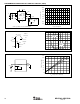
SWITCHING WAVEFORMS
Typical at +25°C, unless otherwise noted.
100ns/Div
1 On
V
A
Input
2V/Div
Output
0.5V/Div
V
AM
4.0V
Address Drive
(V
A
)
Output
50% 50%
t
OPEN
0V
MPC508A
(1)
GND
In 2 Thru In 7
In 1
In 8
Out
A
2
A
1
A
0
En
1kΩ
50Ω
+5V
+4.0V
12.5pF
V
A
V
OUT
NOTE: (1) Similar connection for MPC509A.
BREAK-BEFORE-MAKE DELAY (t
OPEN
)
ENABLE DELAY (t
ON
(EN), t
OFF
(EN))
100ns/Div
Output
2V/Div
MPC508A
(1)
GND
In 2 Thru In 8
In 1
Out
A
2
A
1
A
0
En
1kΩ
+10V
12.5pF
NOTE:
(
1
)
Similar connection for MPC509A.
50Ω
V
A
Enable Drive
V
AM
4.0V
50%
90%
90%
0V
Output
t
ON
(EN)
t
OFF
(EN)
Enable Drive
2V/Div
Factors which will degrade multiplexer and system DC CMR
are:
• Amplifier bias current and differential impedance mis-
match
• Load impedance mismatch
• Multiplexer impedance and leakage current mismatch
• Load and source common-mode impedance
AC CMR roll off is determined by the amount of common-
mode capacitances (absolute and mismatch) from each signal
line to ground. Larger capacitances will limit CMR at higher
frequencies; thus, if good CMR is desired at higher frequen-
cies, the common-mode capacitances and unbalance of sig-
nal lines and multiplexer-to-amplifier wiring must be mini-
mized. Use twisted-shielded-pair signal lines wherever pos-
sible.