
Datasheet


DIN2
DIN1
DOUT2
DOUT1
Auto-Power-Down Plus
INVALID
RIN1
RIN2
FORCEOFF
FORCEON
ROUT1
ROUT2
13
12
20
14
15
10
17
8
11
16
9
5 k
5 k
Ω
Ω
READY
1
MAX3318E
www.ti.com
SLLS741A –JUNE 2006–REVISED OCTOBER 2013
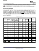
LOGIC DIAGRAM (POSITIVE LOGIC)
TERMINAL FUNCTIONS
TERMINAL
DESCRIPTION
NAME NO.
C1+ 2 Positive voltage-doubler charge-pump capacitor
C1– 4 Negative voltage-doubler charge-pump capacitor
C2+ 5 Positive inverting charge-pump capacitor
C2– 6 Negative inverting charge-pump capacitor
DIN 12, 13 CMOS driver inputs
DOUT 8, 17 RS-232 driver outputs
Force-off input, active low. Drive low to power down transmitters and charge pump. This overrides auto power
FORCEOFF 20
down and FORCEON (see Function Table).
Force-on input, active high. Drive high to override auto power down, keeping transmitters on (FORCEOFF
FORCEON 14
must be high) (see Function Table).
GND 18 Ground
Valid signal detector output, active low. A logic high indicates that a valid RS-232 level is present on a receiver
INVALID 11
input.
Ready to transmit output, active high. READY is enabled high when V– goes below –3.5 V and the device is
READY 1
ready to transmit.
RIN 9, 16 RS-232 receiver inputs
ROUT 10, 15 CMOS receiver outputs
V+ 3 2 × V
CC
generated by the charge pump
V– 7 –2 × V
CC
generated by the charge pump
V
CC
19 2.25-V to 3-V single-supply voltage
Copyright © 2006–2013, Texas Instruments Incorporated Submit Documentation Feedback 3
Product Folder Links: MAX3318E