
Datasheet


±
SLLS350L − APRIL 1999 − REVISED MARCH 2004
8
POST OFFICE BOX 655303 • DALLAS, TEXAS 75265
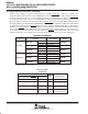
PARAMETER MEASUREMENT INFORMATION
50 Ω
TEST CIRCUIT VOLTAGE WAVEFORMS
0 V
3 V
Output
Input
V
OL
V
OH
t
PLH
Generator
(see Note B)
R
L
3 V
FORCEOFF
RS-232
Output
t
PHL
C
L
(see Note A)
NOTES: A. C
L
includes probe and jig capacitance.
B. The pulse generator has the following characteristics: PRR = 250 kbit/s, Z
O
= 50 Ω, 50% duty cycle, t
r
≤ 10 ns, t
f
≤ 10 ns.
50%
50%
1.5 V
1.5 V
Figure 2. Driver Pulse Skew
TEST CIRCUIT VOLTAGE WAVEFORMS
50 Ω
−3 V
3 V
Output
Input
V
OL
V
OH
t
PHL
Generator
(see Note B)
t
PLH
Output
C
L
(see Note A)
3 V or 0 V
FORCEON
NOTES: A. C
L
includes probe and jig capacitance.
B. The pulse generator has the following characteristics: Z
O
= 50 Ω, 50% duty cycle, t
r
≤ 10 ns, t
f
≤ 10 ns.
3 V
FORCEOFF
1.5 V 1.5 V
50% 50%
Figure 3. Receiver Propagation Delay Times
TEST CIRCUIT
50 Ω
Generator
(see Note B)
3 V or 0 V
3 V or 0 V
FORCEON
FORCEOFF
NOTES: A. C
L
includes probe and jig capacitance.
B. The pulse generator has the following characteristics: Z
O
= 50 Ω, 50% duty cycle, t
r
≤ 10 ns, t
f
≤ 10 ns.
C. t
PLZ
and t
PHZ
are the same as t
dis
.
D. t
PZL
and t
PZH
are the same as t
en
.
R
L
S1
V
CC
GND
C
L
(see Note A)
Output
VOLTAGE WAVEFORMS
Output
V
OL
V
OH
t
PZH
(S1 at GND)
3 V
0 V
0.3 V
Output
Input
0.3 V
1.5 V 1.5 V
50%
t
PHZ
(S1 at GND)
t
PLZ
(S1 at V
CC
)
50%
t
PZL
(S1 at V
CC
)
Figure 4. Receiver Enable and Disable Times