
Datasheet


±
SLLS408G − JANUARY 2000 − REVISED MARCH 2004
4
POST OFFICE BOX 655303 • DALLAS, TEXAS 75265
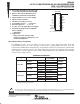
DRIVER SECTION
electrical characteristics over recommended ranges of supply voltage and operating free-air
temperature (unless otherwise noted) (see Note 4 and Figure 5)
PARAMETER TEST CONDITIONS MIN TYP
†
MAX UNIT
V
OH
High-level output voltage DOUT at R
L
= 3 kΩ to GND, DIN = GND 5 5.4 V
V
OL
Low-level output voltage DOUT at R
L
= 3 kΩ to GND, DIN = V
CC
−5 −5.4 V
I
IH
High-level input current V
I
= V
CC
±0.01 ±1 µA
I
IL
Low-level input current V
I
at GND ±0.01 ±1 µA
V
CC
= 3.6 V,
V
O
= 0 V
I
OS
Short-circuit output current
‡
V
CC
= 3.6 V, V
O
= 0 V
±35
±60
mA
I
OS
Short-circuit output current
‡
V
CC
= 5.5 V, V
O
= 0 V
±35 ±60 mA
r
o
Output resistance V
CC
, V+, and V− = 0 V, V
O
= ±2 V 300 10M Ω
I
off
Output leakage current
PWRDOWN = GND,
V
CC
= 3 V to 3.6 V
V
O
= ±12 V,
±25
µA
I
off
Output leakage current
PWRDOWN = GND,
V
CC
= 4.5 V to 5.5 V
V
O
= ±10 V,
±25
µ
A
†
All typical values are at V
CC
= 3.3 V or V
CC
= 5 V, and T
A
= 25°C.
‡
Short-circuit durations should be controlled to prevent exceeding the device absolute power-dissipation ratings, and not more than one output
should be shorted at a time.
NOTE 4: Test conditions are C1−C4 = 0.1 µF at V
CC
= 3.3 V ± 0.3 V; C1 = 0.047 µF, C2−C4 = 0.33 µF at V
CC
= 5 V ± 0.5 V.
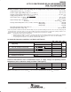
switching characteristics over recommended ranges of supply voltage and operating free-air
temperature (unless otherwise noted) (see Note 4 and Figure 5)
PARAMETER TEST CONDITIONS MIN TYP
†
MAX UNIT
Maximum data rate
C
L
= 1000 pF,
R
L
= 3 k
Ω,
150
250
kbit/s
Maximum data rate
C
L
= 1000 pF,
One DOUT switching,
R
L
= 3 kΩ
,
See Figure 1
150
250 kbit/s
t
sk(p)
Pulse skew
§
C
L
= 150 pF to 2500 pF,
See Figure 2
R
L
= 3 kΩ to 7 kΩ,
300 ns
SR(tr)
Slew rate, transition region
R
L
= 3 k
Ω
to 7 k
Ω
,
C
L
= 150 pF to 1000 pF 6 30
V/µs
SR(tr)
Slew rate, transition region
(See Figure 1)
R
L
= 3 kΩ to 7 kΩ,
V
CC
= 3.3 V
C
L
= 150 pF to 2500 pF 4 30
V/
µ
s
†
All typical values are at V
CC
= 3.3 V or V
CC
= 5 V, and T
A
= 25°C.
§
Pulse skew is defined as |t
PLH
− t
PHL
| of each channel of the same device.
NOTE 4: Test conditions are C1−C4 = 0.1 µF at V
CC
= 3.3 V ± 0.3 V; C1 = 0.047 µF, C2−C4 = 0.33 µF at V
CC
= 5 V ± 0.5 V.