
Datasheet


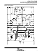


LT1014, LT1014A, LT1014D
QUAD PRECISION OPERATIONAL AMPLIFIERS
SLOS039D − JULY 1989 − REVISED AUGUST 2009
7
POST OFFICE BOX 655303 • DALLAS, TEXAS 75265
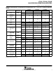
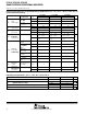
electrical characteristics at specified free-air temperature, V
CC
±
= ±15 V, V
IC
= 0 (unless otherwise
noted)
PARAMETER
TEST CONDITIONS
T
†
LT1014I LT1014DI
UNIT
PARAMETER TEST CONDITIONS
T
A
†
MIN
TYP
‡
MAX MIN
TYP
‡
MAX
UNIT
V
Input offset voltage
R 50 Ω
25°C 60 300 200 800
V
V
IO
Input offset voltage R
S
= 50 Ω
Full range 550 1000
µV
a
V
IO
Temperature coeficient
of input offset voltage
Full range 0.4 2.5 0.7 5 µV/°C
Long-term drift
of input offset voltage
25°C 0.5 0.5 µV/mo
I
Input offset current
25°C 0.15 1.5 0.15 1.5
nA
I
IO
Input offset current
Full range 2.8 2.8
nA
I
Input bias current
25°C −12 −30 −12 −30
nA
I
IB
Input bias current
Full range −38 −38
nA
V
ICR
Common-mode
input voltage range
25°C
−15
to
13.5
−15.3
to
13.8
−15
to
13.5
−15.3
to
13.8
V
V
ICR
input voltage range
Full range
−15
to 13
−15
to 13
V
V
Maximum peak
R 2kΩ
25°C ±12.5 ±14 ±12.5 ±14
V
V
OM
Maximum
peak
output voltage swing
R
L
= 2 kΩ
Full range ±12 ±12
V
L i l diff ti l
V
O
= ±10 V, R
L
= 600 Ω 25°C 0.5 2 0.5 2
A
VD
Large-signal differential
voltage amplification
V ±10 V
R 2kΩ
25°C 1.2 8 1.2 8
V/µV
A
VD
vo
lt
age amp
lifi
ca
ti
on
V
O
= ±10 V, R
L
= 2 kΩ
Full range
0.7 0.7
V/µV
CMRR
Common-mode
V 15Vto135V
25°C 97 117 97 117
dB
CMRR
Common mode
rejection ratio
V
IC
= −15 V to 13.5 V
Full range 94 94
dB
k
Supply-voltage
rejection ratio
V ±2Vto±18 V
25°C 100 117 100 117
dB
k
SVR
rejection ratio
(∆V
CC
/∆V
IO
)
V
CC
±
= ±2 V to ±18 V
Full range 97 97
dB
Channel separation V
O
= ±10 V, R
L
= 2 kΩ 25°C 120 137 120 137 dB
r
id
Differential
input resistance
25°C 70 300 70 300 MΩ
r
ic
Common-mode
input resistance
25°C 4 4 GΩ
I
Suppl
y
current
25°C 0.35 0.55 0.35 0.55
mA
I
CC
Supply
current
per amplifier
Full range 0.6 0.6
mA
†
Full range is −40°C to 105°C.
‡
All typical values are at T
A
= 25°C.