
Datasheet


LP3985
SNVS087AC –OCTOBER 2000–REVISED MAY 2013
www.ti.com
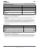
Electrical Characteristics
Unless otherwise specified: V
IN
= V
OUT(nom)
+ 0.5V, C
IN
= 1 µF, I
OUT
= 1mA, C
OUT
= 1 µF, C
BYPASS
= 0.01µF. Typical values and
limits appearing in standard typeface are for T
J
= 25°C. Limits appearing in boldface type apply over the entire junction
temperature range for operation, −40°C to +125°C.
(1)(2)
Limit
Symbol Parameter Conditions Typ Units
Min Max
Output Voltage I
OUT
= 1mA −2 2 % of
Tolerance −3 3 V
OUT(nom)
Line Regulation Error V
IN
= (V
OUT(nom)
+ 0.5V) to 6.0V,
For 4.7 to 5.0 options −0.19 0.19 %/V
ΔV
OUT
For all other options −0.1 0.1
Load Regulation Error
(3)
I
OUT
= 1 mA to 150 mA 0.0025 0.005
LP3985IM5 (SOT23-5)
%/mA
LP3985 (DSBGA) 0.0004 0.002
Output AC Line Regulation V
IN
= V
OUT(nom)
+ 1V, 1.5
mV
P-P
I
OUT
= 150 mA (Figure 5)
V
IN
= V
OUT(nom)
+ 0.2V, 50
f = 1 kHz,
I
OUT
= 50 mA (Figure 6)
PSRR Power Supply Rejection Ratio dB
V
IN
= V
OUT(nom)
+ 0.2V, 40
f = 10 kHz,
I
OUT
= 50 mA (Figure 6)
I
Q
Quiescent Current V
EN
= 1.4V, I
OUT
= 0 mA
For 4.7 to 5.0 options 100 165
For all other options 85 150
V
EN
= 1.4V, I
OUT
= 0 to 150 mA µA
For 4.7 to 5.0 options 155 250
For all other options 140 200
V
EN
= 0.4V 0.003 1.5
Dropout Voltage
(4)
I
OUT
= 1 mA 0.4 2
I
OUT
= 50 mA 20 35
mV
I
OUT
= 100 mA 45 70
I
OUT
= 150 mA 60 100
I
SC
Short Circuit Current Limit Output Grounded 600
mA
(Steady State)
I
OUT(PK)
Peak Output Current V
OUT
≥ V
OUT(nom)
- 5% 550 300 mA
T
ON
Turn-On Time
(5)
C
BYPASS
= 0.01 µF 200 µs
e
n
Output Noise Voltage
(6)
BW = 10 Hz to 100 kHz, 30 µVrms
C
OUT
= 1µF
Output Noise Density C
BP
= 0 230 nV/ √Hz
I
EN
Maximum Input Current at EN V
EN
= 0.4 and V
IN
= 6.0 ±1 nA
V
IL
Maximum Low Level Input Voltage V
IN
= 2.5 to 6.0V 0.4 V
at EN
V
IH
Minimum High Level Input Voltage V
IN
= 2.5 to 6.0V 1.4 V
at EN
Thermal Shutdown Temperature 160 °C
TSD
Thermal Shutdown Hysteresis 20 °C
(1) All limits are verified. All electrical characteristics having room-temperature limits are tested during production with T
J
= 25°C or
correlated using Statistical Quality Control (SQC) methods. All hot and cold limits are specified by correlating the electrical
characteristics to process and temperature variations and applying statistical process control.
(2) The target output voltage, which is labeled V
OUT(nom)
, is the desired voltage option.
(3) An increase in the load current results in a slight decrease in the output voltage and vice versa.
(4) Dropout voltage is the input-to-output voltage difference at which the output voltage is 100mV below its nominal value. This specification
does not apply for input voltages below 2.5V.
(5) Turn-on time is time measured between the enable input just exceeding V
IH
and the output voltage just reaching 95% of its nominal
value.
(6) The output noise varies with output voltage option. The 30µVrms is measured with 2.5V voltage option. To calculate an approximated
output noise for other options, use the equation: (30µVrms)(X)/2.5, where X is the voltage option value.
6 Submit Documentation Feedback Copyright © 2000–2013, Texas Instruments Incorporated
Product Folder Links: LP3985