
Datasheet


LP3962, LP3965
www.ti.com
SNVS066H –MAY 2000–REVISED APRIL 2013
where I
GND
is the operating ground current of the device (specified under Electrical Characteristics).
The maximum allowable temperature rise (T
Rmax
) depends on the maximum ambient temperature (T
Amax
) of the
application, and the maximum allowable junction temperature(T
Jmax
):
T
Rmax
= T
Jmax
− T
Amax
The maximum allowable value for junction to ambient Thermal Resistance, θ
JA
, can be calculated using the
formula:
θ
JA
= T
Rmax
/ P
D
LP3962 and LP3965 are available in TO-220, SFM/TO-263, and SOT-223 packages. The thermal resistance
depends on amount of copper area or heat sink, and on air flow. If the maximum allowable value of θ
JA
calculated above is ≥ 60 °C/W for TO-220 package, ≥60 °C/W for SFM/TO-263 package, and ≥ 140 °C/W for
SOT-223 package, no heatsink is needed since the package can dissipate enough heat to satisfy these
requirements. If the value for allowable θ
JA
falls below these limits, a heat sink is required.
HEATSINKING TO-220 PACKAGES
The thermal resistance of a TO-220 package can be reduced by attaching it to a heat sink or a copper plane on
a PC board. If a copper plane is to be used, the values of θ
JA
will be same as shown in next section for SFM/TO-
263 package.
The heatsink to be used in the application should have a heatsink to ambient thermal resistance,
θ
HA
≤ θ
JA
− θ
CH
− θ
JC
.
In this equation, θ
CH
is the thermal resistance from the junction to the surface of the heat sink and θ
JC
is the
thermal resistance from the junction to the surface of the case. θ
JC
is about 3°C/W for a TO-220 package. The
value for θ
CH
depends on method of attachment, insulator, etc. θ
CH
varies between 1.5°C/W to 2.5°C/W. If the
exact value is unknown, 2°C/W can be assumed.
HEATSINKING SFM/TO-263 AND SOT-223 PACKAGES
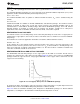
The SFM/TO-263 and SOT-223 packages use the copper plane on the PCB as a heatsink. The tab of these
packages are soldered to the copper plane for heat sinking. Figure 24 shows a curve for the θ
JA
of SFM/TO-263
package for different copper area sizes, using a typical PCB with 1 ounce copper and no solder mask over the
copper area for heat sinking.
Figure 24. θ
JA
vs Copper(1 Ounce) Area for SFM/TO-263 package
As shown in the figure, increasing the copper area beyond 1 square inch produces very little improvement. The
minimum value for θ
JA
for the SFM/TO-263 packag mounted to a PCB is 32°C/W.
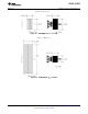
Figure 25 shows the maximum allowable power dissipation for SFM/TO-263 packages for different ambient
temperatures, assuming θ
JA
is 35°C/W and the maximum junction temperature is 125°C.
Copyright © 2000–2013, Texas Instruments Incorporated Submit Documentation Feedback 15
Product Folder Links: LP3962 LP3965