
Datasheet


LP3852, LP3855
SNVS174G –FEBRUARY 2003–REVISED APRIL 2013
www.ti.com
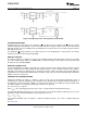
Figure 24. Improving remote load regulation using LP3855
SHUTDOWN OPERATION
A CMOS Logic low level signal at the shutdown ( SD) pin will turn-off the regulator. Pin SD must be actively
terminated through a 10kΩ pull-up resistor for a proper operation. If this pin is driven from a source that actively
pulls high and low (such as a CMOS rail to rail comparator), the pull-up resistor is not required. This pin must be
tied to Vin if not used.
The Shutdown (SD) pin threshold has no voltage hysteresis. If the Shutdown pin is actively driven, the voltage
transition must rise and fall cleanly and promptly.
DROPOUT VOLTAGE
The dropout voltage of a regulator is defined as the minimum input-to-output differential required to stay within
2% of the nominal output voltage. For CMOS LDOs, the dropout voltage is the product of the load current and
the Rds(on) of the internal MOSFET.
REVERSE CURRENT PATH
The internal MOSFET in LP3852 and LP3855 has an inherent parasitic diode. During normal operation, the input
voltage is higher than the output voltage and the parasitic diode is reverse biased. However, if the output is
pulled above the input in an application, then current flows from the output to the input as the parasitic diode gets
forward biased. The output can be pulled above the input as long as the current in the parasitic diode is limited to
200mA continuous and 1A peak.
POWER DISSIPATION/HEATSINKING
LP3852 and LP3855 can deliver a continuous current of 1.5A over the full operating temperature range. A
heatsink may be required depending on the maximum power dissipation and maximum ambient temperature of
the application. Under all possible conditions, the junction temperature must be within the range specified under
operating conditions. The total power dissipation of the device is given by:
P
D
= (V
IN
−V
OUT
)I
OUT
+ (V
IN
)I
GND
where I
GND
is the operating ground current of the device (specified under Electrical Characteristics).
The maximum allowable temperature rise (T
Rmax
) depends on the maximum ambient temperature (T
Amax
) of the
application, and the maximum allowable junction temperature (T
Jmax
):
T
Rmax
= T
Jmax
− T
Amax
The maximum allowable value for junction to ambient Thermal Resistance, θ
JA
, can be calculated using the
formula:
θ
JA
= T
Rmax
/ P
D
14 Submit Documentation Feedback Copyright © 2003–2013, Texas Instruments Incorporated
Product Folder Links: LP3852 LP3855