
Datasheet


LP2950-N, LP2951-N
www.ti.com
SNVS764N –JANUARY 2000–REVISED MAY 2013
These devices have limited built-in ESD protection. The leads should be shorted together or the device placed in conductive foam
during storage or handling to prevent electrostatic damage to the MOS gates.
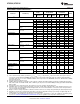
ABSOLUTE MAXIMUM RATINGS
(1)(2)
Input Supply Voltage - SHUTDOWN Input Voltage Error Comparator Output Voltage
(3)
−0.3 to +30V
FEEDBACK Input Voltage
(3)(4)
−1.5 to +30V
Power Dissipation Internally Limited
Junction Temperature (T
J
) +150°C
Ambient Storage Temperature −65° to +150°C
Soldering Dwell Time, Temperature Wave 4 seconds, 260°C
Infrared 10 seconds, 240°C
Vapor Phase 75 seconds, 219°C
ESD Rating Human Body Model
(5)
2500V
(1) Absolute Maximum Ratings are limits beyond which damage to the device may occur. Operating Ratings are conditions under which
operation of the device is specified. Operating Ratings do not imply ensured performance limits. For ensured performance limits and
associated test conditions, see the Electrical Characteristics tables.
(2) If Military/Aerospace specified devices are required, please contact the Texas Instruments Sales Office/Distributors for availability and
specifications.
(3) May exceed input supply voltage.
(4) When used in dual-supply systems where the output terminal sees loads returned to a negative supply, the output voltage should be
diode-clamped to ground.
(5) Human Body Model (HBM) is 1.5 kΩ in series with 100 pF; LP2950-N passes 2.5 kV (HBM) ESD; LP2951-N passes 2.5 kV (HBM)
except: Feedback pin passes 1kV (HBM) and Shutdown pin passes 2kV (HBM).
OPERATING RATINGS
(1)
Maximum Input Supply Voltage 30V
LP2950AC-XX, LP2950C-XX −40° to +125°C
Junction Temperature Range (T
J
)
(2)
LP2951 −55° to +150°C
LP2951AC-XX, LP2951C-XX −40° to +125°C
(1) Absolute Maximum Ratings are limits beyond which damage to the device may occur. Operating Ratings are conditions under which
operation of the device is specified. Operating Ratings do not imply ensured performance limits. For ensured performance limits and
associated test conditions, see the Electrical Characteristics tables.
(2) The junction-to-ambient thermal resistances are as follows: 180°C/W and 160°C/W for the TO-92 package with 0.40 inch and 0.25 inch
leads to the printed circuit board (PCB) respectively, 105°C/W for the molded PDIP (P), 130°C/W for the ceramic DIP (NAB), 160°C/W
for the molded plastic SOIC (D), 200°C/W for the molded plastic VSSOP (DGK), and 160°C/W for the metal can package (LMC). The
above thermal resistances for the P, NAB, D, and DGK packages apply when the package is soldered directly to the PCB. Junction-to-
case thermal resistance for the LMC package is 20°C/W. Junction-to-case thermal resistance for the PFM package is 5.4°C/W. The
value of θ
JA
for the WSON package is typically 51°C/W but is dependent on the PCB trace area, trace material, and the number of
layers and thermal vias. For details of thermal resistance and power dissipation for the WSON package, refer to Application Note AN-
1187 (literature number SNOA401).
Copyright © 2000–2013, Texas Instruments Incorporated Submit Documentation Feedback 3
Product Folder Links: LP2950-N LP2951-N