
Datasheet


LMZ31710
SNVS987A –JULY 2013–REVISED JULY 2013
www.ti.com
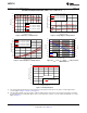
Table 2. PIN DESCRIPTIONS
TERMINAL
DESCRIPTION
NAME NO.
2 Zero volt reference for the analog control circuit. These pins are not connected together internal to the
AGND device and must be connected to one another using an AGND plane of the PCB. These pins are associated
23
with the internal analog ground (AGND) of the device. See Layout Recommendations.
20
21
This is the return current path for the power stage of the device. Connect these pins to the load and to the
PGND 31
bypass capacitors associated with PVIN and VOUT.
32
33
Input bias voltage pin. Supplies the control circuitry of the power converter. Connect this pin to the input bias
VIN 3
supply. Connect bypass capacitors between this pin and PGND.
1
11
Input switching voltage. Supplies voltage to the power switches of the converter. Connect these pins to the
PVIN 12
input supply. Connect bypass capacitors between these pins and PGND.
39
40
34
35
36
Output voltage. These pins are connected to the internal output inductor. Connect these pins to the output
VOUT
load and connect external bypass capacitors between these pins and PGND.
37
38
41
10
13
14
15
Phase switch node. These pins must be connected to one another using a small copper island under the
PH 16 device for thermal relief. Do not place any external component on these pins or tie them to a pin of another
function.
17
18
19
42
5
Do Not Connect. Do not connect these pins to AGND, to another DNC pin, or to any other voltage. These
DNC 9
pins are connected to internal circuitry. Each pin must be soldered to an isolated pad.
24
Current share pin. Connect this pin to other LMZ31710 device's ISHARE pin when paralleling multple
ISHARE 25 LMZ31710 devices. When unused, treat this pin as a Do Not Connect (DNC) and leave it isolated from all
other signals or ground.
Over current protection select pin. Leave this pin open for hiccup mode operation. Connect this pin to AGND
OCP_SEL 4
for cycle-by-cycle operation. See Overcurrent Protection for more details.
Current limit pin. Leave this pin open for full current limit threshold. Connect this pin to AGND to reduce the
ILIM 6
current limit threshold by appoximately 3 A.
SYNC_OUT 7 Synchronization output pin. Provides a 180° out-of-phase clock signal.
Power Good flag pin. This open drain output asserts low if the output voltage is more than approximately
PWRGD 8
±6% out of regulation. A pull-up resistor is required.
This pin is connected to an internal frequency setting resistor which sets the default switching frequency. An
RT/CLK 22 external resistor can be connected from this pin to AGND to increase the frequency. This pin can also be
used to synchronize to an external clock.
VADJ 26 Connecting a resistor between this pin and AGND sets the output voltage.
Remote sense connection. This pin must be connected to VOUT at the load or at the device pins. Connect
SENSE+ 27
this pin to VOUT at the load for improved regulation.
6 Submit Documentation Feedback Copyright © 2013, Texas Instruments Incorporated
Product Folder Links: LMZ31710