
Datasheet

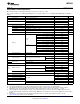


1000 10000 100000 500000
−40
−30
−20
−10
0
10
20
30
40
−120
−90
−60
−30
0
30
60
90
120
Frequency (Hz)
Gain (dB)
Phase (°)
Gain
Phase
G000
0
0.3
0.6
0.9
1.2
1.5
1.8
0 1 2 3 4 5 6
Output Current (A)
Power Dissipation (W)
V
OUT
= 3.3 V, f
SW
= 1 MHz
V
OUT
= 2.5 V, f
SW
= 1 MHz
V
OUT
= 1.8 V, f
SW
= 1 MHz
V
OUT
= 1.2 V, f
SW
= 750 kHz
V
OUT
= 0.8 V, f
SW
= 650 kHz
G000
20
30
40
50
60
70
80
90
0 1 2 3 4 5 6
Output Current (A)
Ambient Temperature (°C)
Natural ConvectionAll Output Voltages
G000
50
55
60
65
70
75
80
85
90
95
100
0 1 2 3 4 5 6
Output Current (A)
Efficiency (%)
V
OUT
= 3.3 V, f
SW
= 1 MHz
V
OUT
= 2.5 V, f
SW
= 1 MHz
V
OUT
= 1.8 V, f
SW
= 1 MHz
V
OUT
= 1.2 V, f
SW
= 750 kHz
V
OUT
= 0.8 V, f
SW
= 650 kHz
G000
9
10
11
12
13
14
15
0 1 2 3 4 5 6
Output Current (A)
Output Voltage Ripple (mV)
V
OUT
= 3.3 V, f
SW
= 1 MHz
V
OUT
= 2.5 V, f
SW
= 1 MHz
V
OUT
= 1.8 V, f
SW
= 1 MHz
V
OUT
= 1.2 V, f
SW
= 750 kHz
V
OUT
= 0.8 V, f
SW
= 650 kHz
G000
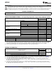
LMZ30606
www.ti.com
SNVS995 –JULY 2013
TYPICAL CHARACTERISTICS (VIN = 5 V)
(1) (2)
Figure 1. Efficiency vs. Output Current Figure 2. Voltage Ripple vs. Output Current
Figure 3. Power Dissipation vs. Output Current Figure 4. Safe Operating Area
Figure 5. V
OUT
= 1.8 V, I
OUT
= 6 A, C
OUT1
= 47 µF ceramic, C
OUT2
= 100 µF POSCAP, f
SW
= 1 MHz
(1) The electrical characteristic data has been developed from actual products tested at 25°C. This data is considered typical for the
converter. Applies to Figure 1, Figure 2, and Figure 3.
(2) The temperature derating curves represent the conditions at which internal components are at or below the manufacturer's maximum
operating temperatures. Derating limits apply to devices soldered directly to a 100 mm × 100 mm double-sided PCB with 1 oz. copper.
Applies to Figure 4.
Copyright © 2013, Texas Instruments Incorporated Submit Documentation Feedback 7
Product Folder Links: LMZ30606