
Datasheet


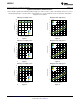


PGND/EP
Connect to AGND
5
AGND
6
AGND
3
SYNC
1
VIN
2
VIN
4
EN
7
FB
SS
9
SH
10
VOUT
11
VOUT
8
V
IN
C
IN
3 x 10 PF
R
FBT
C
FF
4.7 nF (OPT)
See Table
C
SS
0.47 PF
(OPT)
R
FBB
See Table
C
OUT
2 x 330 PF
LMZ22010
SH
SS
FB
SYNC
EN
PGND
V
OUT
5V 5.62k 1.07k 7...20V
V
OUT
R
FBT
R
FBB
V
IN
Range
3.3V 3.32k 1.07k 6...20V
2.5V 2.26k 1.07k 6...20V
1.8V 1.87k 1.50k 6...20V
1.5V 1.00k 1.13k 6...20V
1.2V 1.07k 2.05k 6...20V
0.8V 0 4.02k 6...20V
AGND
6V 15.4k 2.37k 8.5...20V
1.0V 1.62k 6.49k 6...20V
Enable
VIN
VOUT
Share
Clock
LMZ22010
www.ti.com
SNVS687G –MARCH 2011–REVISED OCTOBER 2013
Simplified Application Schematic
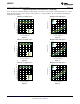
Connection Diagram
Figure 5. Top View
11-Lead PFM
Pin Descriptions
Pin Name Description
1, 2 VIN Input supply — Nominal operating range is 6V to 20V . A small amount of internal capacitance is contained within the
package assembly. Additional external input capacitance is required between this pin and the exposed pad (PGND).
3 SYNC Synchronization — Apply a CMOS logic level square wave whose frequency is between 314 kHz and 600 kHz to
synchronize the PWM operating frequency to an external frequency source. When not using synchronization this pin
must be tied to ground. The module free running PWM frequency is 359 kHz (Typ).
4 EN Enable — Input to the precision enable comparator. Rising threshold is 1.274V typical. Once the module is enabled, a
13 uA source current is internally activated to facilitate programmable hysteresis.
5, 6 AGND Analog Ground — Reference point for all stated voltages. Must be externally connected to PGND(EP).
7 FB Feedback — Internally connected to the regulation amplifier and over-voltage comparator. The regulation reference
point is 0.795V at this input pin. Connect the feedback resistor divider between VOUT and AGND to set the output
voltage.
8 SS Soft-Start/Track Input — To extend the 1.6 mSec internal soft-start connect an external soft start capacitor. For tracking
connect to an external resistive divider connected to a higher priority supply rail. See Design Steps for the LMZ22010
Application section.
9 SH Share — Connect this pin to the share pin of other LMZ22010 modules to share the load between the devices. One
device should be configured as the master by connecting FB normally. All other devices should be configured as slaves
by leaving their respective FB pins floating. Leave SH floating if current sharing is not used. Do Not Ground. See Design
Steps for the LMZ22010 Application section.
10, 11 VOUT Output Voltage — Output from the internal inductor. Connect the output capacitor between this pin and exposed pad
(PGND).
Copyright © 2011–2013, Texas Instruments Incorporated Submit Documentation Feedback 3
Product Folder Links: LMZ22010