
Datasheet


C
IN
1
R
FBT
C
SS
R
FBB
SH
SS
FB
SYNC
EN
PGND
V
OUT
AGND
VIN
VOUT
Share
Clk
LMZ22010
LOAD
V
IN
C
IN
6
(OPT)
C
O
3,4
C
IN5
(OPT)
+
C
IN
2,3,4
C
O
1
(OPT)
C
O
2
(OPT)
C
O
5
(OPT)
R
SYNC
R
ENB
R
ENT
D1
5.1V
(OPT)
'i
L
=
(V
IN
- V
OUT
) x D
L x f
SW
I
DCB
=
(V
IN
- V
OUT
) x D
2 x L x f
SW
LMZ22010
www.ti.com
SNVS687G –MARCH 2011–REVISED OCTOBER 2013
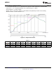
Figure 57. CCM and DCM Operating Modes
V
IN
= 12V, V
O
= 3.3V, I
O
= 3A/0.3A
The approximate formula for determining the DCM/CCM boundary is as follows:
(17)
The inductor internal to the module is 2.2 μH. This value was chosen as a good balance between low and high
input voltage applications. The main parameter affected by the inductor is the amplitude of the inductor ripple
current (Δi
L
). Δi
L
can be calculated with:
(18)
Where V
IN
is the maximum input voltage and f
SW
is typically 359 kHz.
If the output current I
OUT
is determined by assuming that I
OUT
= I
L
, the higher and lower peak of Δi
L
can be
determined.
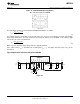
Typical Application Schematic Diagram and BOM
Figure 58.
Copyright © 2011–2013, Texas Instruments Incorporated Submit Documentation Feedback 23
Product Folder Links: LMZ22010