
Datasheet


V
OUT
= 0.8V x
R
fbt
+ R
fbb
R
fbb
C
o
8
42 µF
C
o
8
2.4A x 0.8V x 2.2 µH x 5V
4 x 2.5V x (5V - 2.5V) x 20mV
I
step
x V
FB
x L x V
IN
4 x V
OUT
x (V
IN
- V
OUT
) x '
Vo_tran
C
O
t
LMZ10503
www.ti.com
SNVS641I –JANUARY 2010–REVISED OCTOBER 2013
(11)
Where I
step
is the peak to peak load step (for this example I
step
= 10% to 90% of the maximum load), V
FB
= 0.8V,
and ΔV
o_tran
is the maximum output voltage deviation, which is ±20 mV.
Therefore the capacitance requirement for the given design parameters is:
(12)
(13)
In this particular design the output capacitance is determined by the load transient requirements.
Table 1 lists some examples of commercially available capacitors that can be used with the LMZ10503.
Table 1. Recommended Output Filter Capacitors
C
O
(µF) Voltage (V), R
ESR
(mΩ) Make Manufacturer Part Number Case Size
22 6.3, < 5 Ceramic, X5R TDK C3216X5R0J226M 1206
47 6.3, < 5 Ceramic, X5R TDK C3216X5R0J476M 1206
47 6.3, < 5 Ceramic, X5R TDK C3225X5R0J476M 1210
47 10.0, < 5 Ceramic, X5R TDK C3225X5R1A476M 1210
100 6.3, < 5 Ceramic, X5R TDK C3225X5R0J107M 1210
100 6.3, 50 Tantalum AVX TPSD157M006#0050 D, 7.5 x 4.3 x 2.9 mm
100 6.3, 25 Organic Polymer Sanyo 6TPE100MPB2 B2, 3.5 x 2.8 x 1.9 mm
150 6.3, 18 Organic Polymer Sanyo 6TPE150MIC2 C2, 6.0 x 3.2 x 1.8 mm
330 6.3, 18 Organic Polymer Sanyo 6TPE330MIL D3L, 7.3 x 4.3 x 2.8 mm
470 6.3, 23 Niobium Oxide AVX NOME37M006#0023 E, 7.3 x 4.3 x 4.1 mm
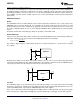
Output Voltage Setting
A resistor divider network from V
OUT
to the FB pin determines the desired output voltage as follows:
(14)
R
fbt
is defined based on the voltage loop requirements and R
fbb
is then selected for the desired output voltage.
Resistors are normally selected as 0.5% or 1% tolerance. Higher accuracy resistors such as 0.1% are also
available.
The feedback voltage (at V
OUT
= 2.5V) is accurate to within -2.5% / +2.5% over temperature and over line and
load regulation. Additionally, the LMZ10503 contains error nulling circuitry to substantially eliminate the feedback
voltage variation over temperature as well as the long term aging effects of the internal amplifiers. In addition the
zero nulling circuit dramatically reduces the 1/f noise of the bandgap amplifier and reference. The manifestation
of this circuit action is that the duty cycle will have two slightly different but distinct operating points, each evident
every other switching cycle.
Loop Compensation
The LMZ10503 preserves flexibility by integrating the control components around the internal error amplifier while
utilizing three small external compensation components from V
OUT
to FB. An integrated type II (two pole, one
zero) voltage-mode compensation network is featured. To ensure stability, an external resistor and small value
capacitor can be added across the upper feedback resistor as a pole-zero pair to complete a type III (three pole,
two zero) compensation network. The compensation components recommended in Table 2 provide type III
compensation at an optimal control loop performance. The typical phase margin is 45° with a bandwidth of 80
kHz. Calculated output capacitance values not listed in Table 2 should be verified before designing into
production. A detailed application note is available to provide verification support, AN-2013 (SNVA417). In
general, calculated output capacitance values below the suggested value will have reduced phase margin and
higher control loop bandwidth. Output capacitance values above the suggested values will experience a lower
Copyright © 2010–2013, Texas Instruments Incorporated Submit Documentation Feedback 11
Product Folder Links: LMZ10503