
Datasheet


LMV931-N, LMV931-N-Q1, LMV932-N, LMV932-N-Q1
LMV934-N, LMV934-N-Q1
SNOS993M –NOVEMBER 2001–REVISED NOVEMBER 2013
www.ti.com
These devices have limited built-in ESD protection. The leads should be shorted together or the device placed in conductive foam
during storage or handling to prevent electrostatic damage to the MOS gates.
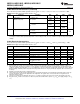
Absolute Maximum Ratings
(1)(2)
Charged Device Model 750V
ESD Tolerance
(3)
Machine Model 200V
Human Body Model 2000V
Supply Voltage (V
+
–V
−
) 6V
Differential Input Voltage ± Supply Voltage
Voltage at Input/Output Pins V
+
+0.3V, V
-
-0.3V
Storage Temperature Range −65°C to 150°C
Junction Temperature
(4)
150°C
For soldering specifications:
See product folder at www.ti.com and http://www.ti.com/lit/SNOA549
(1) Absolute Maximum Ratings indicate limits beyond which damage to the device may occur. Operating Ratings indicate conditions for
which the device is intended to be functional, but specific performance is not guaranteed. For guaranteed specifications and the test
conditions, see the Electrical Characteristics.
(2) If Military/Aerospace specified devices are required, please contact the Texas Instruments Sales Office / Distributors for availability and
specifications.
(3) Human Body Model, applicable std. MIL-STD-883, Method 3015.7. Machine Model, applicable std. JESD22-A115-A (ESD MM std. of
JEDEC)Field-Induced Charge-Device Model, applicable std. JESD22-C101-C (ESD FICDM std. of JEDEC).
(4) The maximum power dissipation is a function of T
J(MAX)
, θ
JA
and T
A
. The maximum allowable power dissipation at any ambient
temperature is P
D
= (T
J(MAX)
– T
A
)/ θ
JA
. All numbers apply for packages soldered directly onto a PC Board.
Operating Ratings
(1)
Supply Voltage Range 1.8V to 5.5V
Temperature Range −40°C to 125°C
5-Pin SC70 414°C/W
5-Pin SOT-23 265°C/W
8-Pin VSSOP 235°C/W
Thermal Resistance (θ
JA
)
8-Pin SOIC 175°C/W
14-Pin TSSOP 155°C/W
14-Pin SOIC 127°C/W
(1) Absolute Maximum Ratings indicate limits beyond which damage to the device may occur. Operating Ratings indicate conditions for
which the device is intended to be functional, but specific performance is not guaranteed. For guaranteed specifications and the test
conditions, see the Electrical Characteristics.
2 Submit Documentation Feedback Copyright © 2001–2013, Texas Instruments Incorporated
Product Folder Links: LMV931-N LMV931-N-Q1 LMV932-N LMV932-N-Q1 LMV934-N LMV934-N-Q1