
Datasheet


LMV851, LMV852, LMV854
www.ti.com
SNOSAW1A –OCTOBER 2007–REVISED MARCH 2013
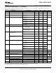
3.3V Electrical Characteristics
(1)
(continued)
Unless otherwise specified, all limits are specified for T
A
= 25°C, V
+
= 3.3V, V
−
= 0V, V
CM
= V
+
/2, and R
L
= 10 kΩ to V
+
/2.
Boldface limits apply at the temperature extremes.
Parameter Test Conditions Min
(2)
Typ
(3)
Max
(2)
Units
I
OS
Input Offset Current 1 pA
CMRR Common Mode Rejection Ratio −0.2V < V
CM
< V
+
- 1.2V 76 92
dB
75 See
(4)
PSRR Power Supply Rejection Ratio 2.7V ≤ V
+
≤ 5.5V, 75 93
dB
V
OUT
= 1V 74
(4)
EMIRR EMI Rejection Ratio, IN+ and IN−
(6)
V
RFpeak
= 100 mV
P
(−20 dBV
P
), 64
f = 400 MHz
V
RFpeak
= 100 mV
P
(−20 dBV
P
), 78
f = 900 MHz
dB
V
RFpeak
= 100 mV
P
(−20 dBV
P
), 87
f = 1800 MHz
V
RFpeak
= 100 mV
P
(−20 dBV
P
), 90
f = 2400 MHz
CMVR Input Common-Mode Voltage Range CMRR ≥ 76 dB −0.2 2.1 V
A
VOL
Large Signal Voltage Gain
(7)
R
L
= 2 kΩ, 100 114
V
OUT
= 0.15V to 1.65V, 97
V
OUT
= 3.15V to 1.65V
dB
R
L
= 10 kΩ, 100 115
V
OUT
= 0.1V to 1.65V, 97
V
OUT
= 3.2V to 1.65V
V
O
Output Swing High, R
L
= 2 kΩ to V
+
/2 31 35
(measured from V
+
) 43
mV
R
L
= 10 kΩ to V
+
/2 7 10
12
Output Swing Low, R
L
= 2 kΩ to V
+
/2 26 32
(measured from V
−
) 43
mV
R
L
= 10 kΩ to V
+
/2 6 11
14
I
O
Output Short Circuit Current Sourcing, V
OUT
= V
CM
, 25 28
V
IN
= 100 mV 20
mA
Sinking, V
OUT
= V
CM
, 28 31
V
IN
= −100 mV 20
I
S
Supply Current LMV851 0.42 0.50
0.58
LMV852 0.79 0.90
mA
1.06
LMV854 1.54 1.67
1.99
SR Slew Rate
(8)
A
V
= +1, V
OUT
= 1 V
PP
, 10% to 90% 4.5 V/μs
GBW Gain Bandwidth Product 8 MHz
Φ
m
Phase Margin 62 deg
e
n
Input-Referred Voltage Noise f = 1 kHz 11
nV/√Hz
f = 10 kHz 10
i
n
Input-Referred Current Noise f = 1 kHz 0.005 pA/√Hz
R
OUT
Closed Loop Output Impedance f = 6 MHz 400 Ω
C
IN
Common-Mode Input Capacitance 11
pF
Differential-Mode Input Capacitance 6
THD+N Total Harmonic Distortion + Noise f = 1 kHz, A
V
= 1, BW = >500 kHz 0.006 %
(6) The EMI Rejection Ratio is defined as EMIRR = 20log ( V
RFpeak
/ΔV
OS
).
(7) The specified limits represent the lower of the measured values for each output range condition.
(8) Number specified is the slower of positive and negative slew rates.
Copyright © 2007–2013, Texas Instruments Incorporated Submit Documentation Feedback 3
Product Folder Links: LMV851 LMV852 LMV854