
Datasheet


V
O
0
V
IN2
V
IN1
V
IN
LMV761, LMV762
SNOS998H –FEBRUARY 2002–REVISED MARCH 2013
www.ti.com
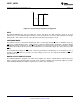
Figure 25. Non-Inverting Comparator Configuration
INPUT
The LMV761/LMV762 have near zero input bias current. This allows very high resistance circuits to be used
without any concern for matching input resistances. This also allows the use of very small capacitors in R-C type
timing circuits. This reduces the cost of the capacitors and amount of board space used.
SHUTDOWN MODE
The LMV761 features a low-power shutdown pin that is activated by driving SD low. In shutdown mode, the
output is in a high impedance state, supply current is reduced to 20nA and the comparator is disabled. Driving
SD high will turn the comparator on. The SD pin should not be left unconnected due to the fact that it is a high
impedance input. When left unconnected, the output will be at an unknown voltage. Also do not three-state the
SD pin.
The maximum input voltage for SD is 5.5V, referred to ground and is not limited by V
CC
. This allows the use of
5V logic to drive SD while V
CC
operates at a lower voltage, such as 3V. The logic threshold limits for SD are
proportional to V
CC
.
BOARD LAYOUT AND BYPASSING
The LMV761/LMV762 is designed to be stable and oscillation free, but it is still important to include the proper
bypass capacitors and ground pickups. Ceramic 0.1μF capacitors should be placed at both supplies to provide
clean switching. Minimize the length of signal traces to reduce stray capacitance.
10 Submit Documentation Feedback Copyright © 2002–2013, Texas Instruments Incorporated
Product Folder Links: LMV761 LMV762