
Datasheet


CLASS AB CONTROL
OUT
V
DD
InP
InM
V
EE
LMV341-N, LMV342-N, LMV344-N
www.ti.com
SNOS990G –APRIL 2002–REVISED MARCH 2013
APPLICATION SECTION
LMV341-N/LMV342-N/LMV344-N
The LMV341-N/LMV342-N/LMV344-N family of amplifiers features low voltage, low power, and rail-to-rail output
operational amplifiers designed for low voltage portable applications. The family is designed using all CMOS
technology. This results in an ultra low input bias current. The LMV341-N has a shutdown option, which can be
used in portable devices to increase battery life.
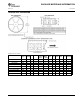
A simplified schematic of the LMV341-N/LMV342-N/LMV344-N family of amplifiers is shown in Figure 44. The
PMOS input differential pair allows the input to include ground. The output of this differential pair is connected to
the Class AB turnaround stage. This Class AB turnaround has a lower quiescent current, compared to regular
turnaround stages. This results in lower offset, noise, and power dissipation, while slew rate equals that of a
conventional turnaround stage. The output of the Class AB turnaround stage provides gate voltage to the
complementary common-source transistors at the output stage. These transistors enable the device to have rail-
to-rail output.
Figure 44. Simplified Schematic
Class AB Turnaround Stage Amplifier
This patented folded cascode stage has a combined class AB amplifier stage, which replaces the conventional
folded cascode stage. Therefore, the class AB folded cascode stage runs at a much lower quiescent current
compared to conventional folded cascode stages. This results in significantly smaller offset and noise
contributions. The reduced offset and noise contributions in turn reduce the offset voltage level and the voltage
noise level at the input of the LMV341-N/LMV342-N/LMV344-N. Also the lower quiescent current results in a high
open-loop gain for the amplifier. The lower quiescent current does not affect the slew rate of the amplifier nor its
ability to handle the total current swing coming from the input stage.
The input voltage noise of the device at low frequencies, below 1kHz, is slightly higher than devices with a BJT
input stage; However the PMOS input stage results in a much lower input bias current and the input voltage
noise drops at frequencies above 1kHz.
Sample and Hold Circuit
The lower input bias current of the LMV341-N results in a very high input impedance. The output impedance
when the device is in shutdown mode is quite high. These high impedances, along with the ability of the
shutdown pin to be derived from a separate power source, make LMV341-N a good choice for sample and hold
circuits. The sample clock should be connected to the shutdown pin of the amplifier to rapidly turn the device on
or off.
Copyright © 2002–2013, Texas Instruments Incorporated Submit Documentation Feedback 13
Product Folder Links: LMV341-N LMV342-N LMV344-N