
Datasheet


LMP8640
LMP8640HV
SNOSB28F –AUGUST 2010–REVISED APRIL 2013
www.ti.com
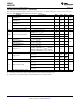
2.7V Electrical Characteristics
(1)
(continued)
Unless otherwise specified, all limits ensured for at T
A
= 25°C, V
S
=V
+
– V
-
, V
SENSE
= +IN-(-IN), V
+
= 2.7V, V
−
= 0V, −2V < V
CM
<
76V, R
L
= 10MΩ. Boldface limits apply at the temperature extremes.
Parameter Test Conditions Min
(2)
Typ
(3)
Max
(2)
Unit
V
CM
=5V, C
L
= 30 pF, R
L
= 1MΩ,
LMP8640-T LMP8640HV-T V
SENSE
=100mVpp,
SR Slew Rate
(7) (5)
1.4 V/µs
LMP8640-F LMP8640HV-F V
SENSE
=40mVpp,
LMP8640-H LMP8640HV-H V
SENSE
=20mVpp,
R
IN
Differential Mode Input Impedance
(5)
5 kΩ
600
V
CM
= 2.1V 420
800
I
S
Supply Current µA
2500
V
CM
= −2V 2000
2750
Maximum Output Voltage V
CM
= 2.1V 2.65 V
LMP8640-T LMP8640HV-T
18.2
V
CM
= 2.1V
V
OUT
LMP8640-F LMP8640HV-F
Minimum Output Voltage 40 mV
V
CM
= 2.1V
LMP8640-H LMP8640HV-H
80
V
CM
= 2.1V
C
LOAD
Max Output Capacitance Load
(5)
30 pF
(7) The number specified is the average of rising and falling slew rates and measured at 90% to 10%.
5V Electrical Characteristics
(1)
Unless otherwise specified, all limits ensured for at T
A
= 25°C, V
S
=V
+
– V
-
, V
SENSE
= +IN-(-IN), V
+
= 5V, V
−
= 0V, −2V < V
CM
<
76V, R
L
= 10MΩ. Boldface limits apply at the temperature extremes.
Parameter Test Conditions Min
(2)
Typ
(3)
Max
(2)
Unit
-900 900
V
OS
Input Offset Voltage V
CM
= 2.1V µV
-1160 1160
TCV
OS
Input Offset Voltage Drift
(4) (5)
V
CM
= 2.1V 2.6 µV/°C
21
I
B
Input Bias Current
(6)
V
CM
= 2.1V 13 µA
28
e
ni
Input Voltage Noise
(5)
f > 10 kHz 117 nV/√Hz
Fixed Gain LMP8640-T
20 V/V
LMP8640HV-T
Fixed Gain LMP8640-F
50 V/V
LMP8640HV-F
Gain A
V
Fixed Gain LMP8640-H
100 V/V
LMP8640HV-H
-0.25 0.25
Gain error V
CM
= 2.1V %
-0.51 0.51
Accuracy over temperature
(5)
−40°C to 125°C, V
CM
=2.1V 26.2 ppm/°C
PSRR Power Supply Rejection Ratio V
CM
= 2.1V, 2.7V < V
+
< 12V, 85 dB
(1) Electrical Table values apply only for factory testing conditions at the temperature indicated. Factory testing conditions result in very
limited self-heating of the device such that T
J
= T
A
. No specification of parametric performance is indicated in the electrical tables under
conditions of internal self-heating where T
J
> T
A
. Absolute Maximum Ratings indicate junction temperature limits beyond which the
device may be permanently degraded, either mechanically or electrically.
(2) Limits are 100% production tested at 25°C. Limits over the operating temperature range are ensured through correlations using
statistical quality control (SQC) method.
(3) Typical values represent the most likely parametric norm at the time of characterization. Actual typical values may vary over time and
will also depend on the application and configuration. The typical values are not tested and are not ensured on shipped production
material.
(4) Offset voltage temperature drift is determined by dividing the change in V
OS
at the temperature extremes by the total temperature
change.
(5) This parameter is ensured by design and/or characterization and is not tested in production.
(6) Positive Bias Current corresponds to current flowing into the device.
4 Submit Documentation Feedback Copyright © 2010–2013, Texas Instruments Incorporated
Product Folder Links: LMP8640 LMP8640HV