
Datasheet

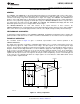


R
i
+IN
-IN
+
-
Preamplifier
Output Buffer
Gain = K2
A1
A2
Gain = 10
OFFSET
Internal
Resistor
100 k:
OUT
Level
shift
1
5
3 4
7
8
R
i
= 100 k:X
G
i
- 20
G
i
G
i
=
R
i
- 100 k:
20 R
i
R
r
= 100 k:X
20 - G
r
G
r
G
r
=
R
r
+ 100 k:
20 R
r
LMP8601, LMP8601-Q1
SNOSAR2E –SEPTEMBER 2008–REVISED MARCH 2013
www.ti.com
(8)
Given a desired value of the reduced gain G
r
, using this equation the required value for R
r
can be calculated
with:
(9)
Increase Gain
Figure 36 shows the configuration that can be used to increase the gain of the LMP8601/LMP8601Q.
R
i
creates positive feedback from the output pin to the input of the buffer amplifier. The positive feedback
increases the gain. The increased gain G
i
becomes:
(10)
From this equation, for a desired value of the gain, the required value of R
i
can be calculated with:
(11)
It should be noted from the equation for the gain G
i
that for large gains R
i
approaches 100 kΩ. In this case, the
denominator in the equation becomes close to zero. In practice, for large gains the denominator will be
determined by tolerances in the value of the external resistor R
i
and the internal 100 kΩ resistor. In this case, the
gain becomes very inaccurate. If the denominator becomes equal to zero, the system will even become instable.
It is recommended to limit the application of this technique to gain values of 50 or smaller.
K2 = 2
Figure 36. Increase Gain
BIDIRECTIONAL CURRENT SENSING
The signal on the A1 and OUT pins is ground-referenced when the OFFSET pin is connected to ground. This
means that the output signal can only represent positive values of the current through the shunt resistor, so only
currents flowing in one direction can be measured. When the offset pin is tied to the positive supply rail, the
signal on the A1 and OUT pins is referenced to a mid-rail voltage which allows bidirectional current sensing.
When the offset pin is connected to a voltage source, the output signal will be level shifted to that voltage divided
by two. In principle, the output signal can be shifted to any voltage between 0 and V
S
/2 by applying twice that
voltage to the OFFSET pin.
16 Submit Documentation Feedback Copyright © 2008–2013, Texas Instruments Incorporated
Product Folder Links: LMP8601 LMP8601-Q1