
Datasheet


LOGIC
I/O LEVELS
VLSER/VHPAR
VHSER/VLPAR
V+
V-
PARALLEL MODE
SERIAL MODE
LMP8358
www.ti.com
SNOSB09B –APRIL 2010–REVISED MARCH 2013
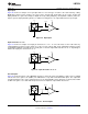
Figure 49. Communication Mode Selection.
PARALLEL CONTROL INTERFACE MODE
The LMP8358 is put into Parallel Mode by setting VLSER/VHPAR > VHSER/VLPAR. The register in the
LMP8358 does not control the settings of the LMP8358 in this mode. Gain and shutdown are set by placing a
high or low logic level on pins 11 (SHDN), 12 (G2), 13 (G1), and 14 (G0), as shown in Table 1 and Table 2. The
logic high and low levels are defined by the voltages on the VLSER/VHPAR and VHSER/VLPAR pins. See the
START UP AND POWER ON RESET section for power on requirements when using the parallel mode.
Table 1. Function of Digital IO Pins, Parallel Mode
Pin Name Description
G0 Gain setting (LSB)
G1 Gain setting
G2 Gain setting (MSB)
SHDN Shutdown (Active High)
VHPAR Positive logic level
VLPAR Negative logic level
Table 2. Pin Levels for Setting Gain, Parallel Mode
G2 G1 G0 Gain Setting Bandwidth Compen-
sation Setting (Auto-
matically
Set)
0 0 0 10x (power-up default) 930 kHz 000b
0 0 1 20x 385 kHz 000b
0 1 0 50x 460 kHz 001b
0 1 1 100x 640 kHz 010b
1 0 0 200x 195 kHz 010b
1 0 1 500x 130 kHz 011b
1 1 0 1000x 89 kHz 011b
1 1 1 User defined 800 kHz 1xxb
SERIAL CONTROL INTERFACE MODE
The LMP8358 is put into Serial Mode by setting VLSER/VHPAR < VHSER/VLPAR. In the Serial Mode the
LMP8358 can be programmed by using pins 11 – 14 as shown in Table 3 and the SPI Timing Diagram. The
LMP8358 contains a 16 bit register which controls the performance of the part. These bits can be changed using
the Serial Mode of communication. The register of the LMP8358 is shown in Table 4. Immediately after power on
the register should be written with the value needed for the application. See the START UP AND POWER ON
RESET section.
Copyright © 2010–2013, Texas Instruments Incorporated Submit Documentation Feedback 21
Product Folder Links: LMP8358