
Datasheet


-
+
FEEDBACK
NETWORK
V
IN_DIFF
V
IN
R
IN
C
IN
INPUT
SWITCHES
V
IN_DIFF
R
IN
R
ON_SWITCH
C
OUT
V
OUT
+
-
V
IN
-
+
FEEDBACK
NETWORK
V
IN_DIFF
V
IN
R
IN
LMP2021, LMP2022
www.ti.com
SNOSAY9E –SEPTEMBER 2008–REVISED MARGH 2013
A
V
*I
BIAS+
*Z
S
- I
BIAS−
*Z
F
(1)
Where A
V
is the closed loop gain of the system and I
BIAS+
and I
BIAS−
denote the positive and negative bias
current, respectively. It is common to show the average of these bias currents in product datasheets. If I
BIAS+
and
I
BIAS−
are not individually specified, use the I
BIAS
value provided in datasheet graphs or tables for this calculation.
For the application circuit shown in Figure 50, the LMP2022 amplifiers each have a gain of 18. With a sensor
impedance of 500Ω for the bridge, and using the above equation, the total error due to the bias current on the
outputs of the LMP2022 amplifier will be less than 200 nV.
SENSOR IMPEDANCE
The sensor resistance, or the resistance connected to the inputs of the LMP2021/LMP2022, contributes to the
total impedance seen by the auto correcting input stage.
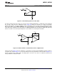
Figure 47. Auto Correcting Input Stage Model
As shown in Figure 47, the sum of R
IN
and R
ON-SWITCH
will form a low pass filter with C
OUT
during correction
cycles. As R
IN
increases, the time constant of this filter increases, resulting in a slower output signal which could
have the effect of reducing the open loop gain, A
VOL
, of the LMP2021/LMP2022. In order to prevent this
reduction in A
VOL
in presence of high impedance sensors or other high resistances connected to the input of the
LMP2021/LMP2022, a capacitor can be placed in parallel to this input resistance. This is shown in Figure 48
Copyright © 2008–2013, Texas Instruments Incorporated Submit Documentation Feedback 19
Product Folder Links: LMP2021 LMP2022