
Datasheet


-
+
FEEDBACK
NETWORK
V
IN_DIFF
V
IN
R
IN
C
IN
INPUT
SWITCHES
V
IN_DIFF
R
IN
R
ON_SWITCH
C
OUT
V
OUT
+
-
C
IN
V
IN
LMP2021, LMP2022
SNOSAY9E –SEPTEMBER 2008–REVISED MARGH 2013
www.ti.com
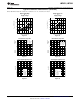
Figure 48. Sensor Impedance with Parallel Capacitance
C
IN
in Figure 48 adds a zero to the low pass filter and hence eliminating the reduction in A
VOL
of the
LMP2021/LMP2022. An alternative circuit to achieve this is shown in Figure 49.
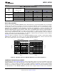
Figure 49. Alternative Sensor Impedance Circuit
TRANSIENT RESPONSE TO FAST INPUTS
On chip continuous auto zero correction circuitry eliminates the 1/f noise and significantly reduces the offset
voltage and offset voltage drift; all of which are very low frequency events. For slow changing sensor signals this
correction is transparent. For excitations which may otherwise cause the output to swing faster than 40 mV/µs,
there are additional considerations which can be viewed two perspectives: for sine waves and for steps.
For sinusoidal inputs, when the output is swinging rail-to-rail on ±2.5V supplies, the auto zero circuitry will
introduce distortions above 2.55 kHz. For smaller output swings, higher frequencies can be amplified without the
auto zero slew limitation as shown in table below. Signals above 20 kHz, are not affected, though normally,
closed loop bandwidth should be kept below 20 kHz so as to avoid aliasing from the auto zero circuit.
V
OUT-PEAK
(V) f
MAX-SINE WAVE
(kHz)
0.32 20
1 6.3
2.5 2.5
For step-like inputs, such as those arising from disturbances to a sensing system, the auto zero slew rate
limitation manifests itself as an extended ramping and settling time, lasting ~100 µs.
DIFFERENTIAL BRIDGE SENSOR
Bridge sensors are used in a variety of applications such as pressure sensors and weigh scales. Bridge sensors
typically have a very small differential output signal. This very small signal needs to be accurately amplified
before it can be fed into an ADC. As discussed in the previous sections, the accuracy of the op amp used as the
ADC driver is essential to maintaining total system accuracy.
The high DC performance of the LMP2021/LMP2022 make these amplifiers ideal choices for use with a bridge
sensor. The LMP2021/LMP2022 have very low input offset voltage and very low input offset voltage drift. The
open loop gain of the LMP2021/LMP2022 is 160 dB.
The on chip EMI rejection filters available on the LMP2021/LMP2022 help remove the EMI interference
introduced to the signal and hence improve the overall system performance.
20 Submit Documentation Feedback Copyright © 2008–2013, Texas Instruments Incorporated
Product Folder Links: LMP2021 LMP2022