
Datasheet


1
10 100
6
7
8
9
10
11
12
13
14
GAIN (dB)
FREQUENCY (MHz)
GAIN
PHASE
V
S
= ±5V
V
OUT
= 2.5 V
PP
R
L
= 5.6:
A
V
= 5
-180
-135
-90
-45
0
45
90
135
180
PHASE
(
°
)
LMH6723, LMH6724, LMH6725
www.ti.com
SNOSA83H –AUGUST 2003–REVISED APRIL 2013
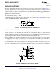
When higher currents are required than a single amplifier can provide, the circuit of Figure 43 can be used.
Although the example circuit was intended for the LMH6725 quad op amp, higher thermal efficiency can be
obtained by using four separate SOIC op amps. Careful attention to a few key components will optimize
performance from this circuit. The first thing to note is that the buffers need slightly higher value feedback
resistors than if the amplifiers were individually configured. As well, R
11
and C
1
provide mid circuit frequency
compensation to further improve stability. The composite amplifier has approximately twice the phase delay of a
single circuit. The larger values of R
8
, R
9
and R
10
, as well as the high frequency attenuation provided by C
1
and
R
11
, ensure that the circuit does not oscillate.
Resistors R
4
, R
5
, R
6
, and R
7
are necessary to ensure even current distribution between the amplifiers. Since they
are inside the feedback loop they have no effect on the gain of the circuit. The circuit shown in Figure 43 has a
gain of 5. The frequency response of this circuit is shown in Figure 44.
Figure 44. Composite Amplifier Frequency Response
LAYOUT CONSIDERATIONS
Whenever questions about layout arise, use the evaluation board as a guide. Evaluation boards are shipped with
sample requests.
To reduce parasitic capacitances ground and power planes should be removed near the input and output pins.
Components in the feedback loop should be placed as close to the device as possible. For long signal paths
controlled impedance lines should be used, along with impedance matching at both ends.
Bypass capacitors should be placed as close to the device as possible. Bypass capacitors from each rail to
ground are applied in pairs. The larger electrolytic bypass capacitors can be located anywhere on the board;
however, the smaller ceramic capacitors should be placed as close to the device as possible.
VIDEO PERFORMANCE
The LMH6723/LMH6724/LMH6725 has been designed to provide good performance with both PAL and NTSC
composite video signals. The LMH6723/LMH6724/LMH6725 is specified for PAL signals. Typically, NTSC
performance is marginally better due to the lower frequency content of the signal. Performance degrades as the
loading is increased; therefore, best performance will be obtained with back terminated loads. The back
termination reduces reflections from the transmission line and effectively masks transmission line and other
parasitic capacitances from the amplifier output stage. Figure 40 shows a typical configuration for driving a 75Ω
cable. The amplifier is configured for a gain of 2 to make up for the 6dB of loss in R
OUT
.
SINGLE 5V SUPPLY VIDEO
With a 5V supply the LMH6723/LMH6724/LMH6725 is able to handle a composite NTSC video signal, provided
that the signal is AC coupled and level shifted so that the signal is centered around V
CC
/2.
Copyright © 2003–2013, Texas Instruments Incorporated Submit Documentation Feedback 17
Product Folder Links: LMH6723 LMH6724 LMH6725