
Datasheet


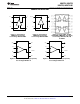


Table Of Contents

1 2 3 4
0
0.01
0.02
0.03
0.04
0.05
DIFFERENTIAL GAIN (%)
VIDEO LOADS (150: EACH)
0
0.01
0.02
0.03
0.04
0.05
DIFFERENTIAL PHASE
(
°
)
PHASE
GAIN
1
10
100
1000
FREQUENCY (MHz)
GAIN (dB)
-8
-7
-6
-5
-4
-3
-2
-1
0
1
2
-225
-180
-135
-90
-45
0
PHASE
(
°
)
A
V
= 1, R
F
= 600:
A
V
= 2, R
F
= 300:
A
V
= 6, R
F
= 200:
GAIN
PHASE
V
O
= 500mV
PP
LMH6714, LMH6720
LMH6722, LMH6722-Q1
SNOSA39G –NOVEMBER 2002–REVISED APRIL 2013
www.ti.com
Typical Performance
Differential Gain and Phase vs. Number of Video Loads
Non-Inverting Small Signal Frequency Response (LMH6714)
Figure 1. Figure 2.
These devices have limited built-in ESD protection. The leads should be shorted together or the device placed in conductive foam
during storage or handling to prevent electrostatic damage to the MOS gates.
Absolute Maximum Ratings
(1)(2)
ESD Tolerance
(3)
Human Body Model 2000V
Machine Model 200V
V
CC
±6.75V
I
OUT
See
(4)
Common Mode Input Voltage ±V
CC
Differential Input Voltage 2.2V
Maximum Junction Temperature +150°C
Storage Temperature Range −65°C to +150°C
Lead Temperature (soldering 10 sec) +300°C
Storage Temperature Range −65°C to +150°C
Shutdown Pin Voltage
(5)
+V
CC
to V
CC
/2-1V
(1) Absolute Maximum Ratings indicate limits beyond which damage to the device may occur. Operating Ratings indicate conditions for
which the device is intended to be functional, but specific performance is not ensured. For specific specifications, see the Electrical
Characteristics tables.
(2) If Military/Aerospace specified devices are required, please contact the Texas Instruments Sales Office/Distributors for availability and
specifications.
(3) Human Body Model, applicable std. MIL-STD-883, Method 3015.7. Machine Model, applicable std. JESD22-A115-A (ESD MM std. of
JEDEC). Field-Induced Charge-Device Model, applicable std. JESD22-C101-C (ESD FICDM std. of JEDEC).
(4) The maximum output current (I
OUT
) is determined by device power dissipation limitations. See the POWER DISSIPATION section for
more details.
(5) The shutdown pin is designed to work between 0 and V
CC
with split supplies (V
CC
= -V
EE
). With single supplies (V
EE
= ground) the
shutdown pin should not be taken below V
CC
/2.
2 Submit Documentation Feedback Copyright © 2002–2013, Texas Instruments Incorporated
Product Folder Links: LMH6714 LMH6720 LMH6722 LMH6722-Q1