
Datasheet


10:
275:
+
-
LMH6553
V
+
V
-
V
O
+
-
V
IN
275:
10:
50:
R
S
= 50:
V
CM
50:
2:1 (TURNS)
A
V
= 9 V/V
1 PF
1 PF
a
2
0
5
1
t
V
OUT(MAX)
SE Unclamped output
4
+V
V
OUT(MAX)
= + 3.7V
V
CLAMP
2*V
CM
± V
CLAMP
SE Unclamped output
t
V
OUT(MIN)
-V
V
OUT(MIN)
= -3.7V
V
CLAMP
2*V
CM
± V
CLAMP
-4
V
CM
= -3
-1
-5
-2
0
V
CM
= 3
LMH6553
SNOSB07H –SEPTEMBER 2008–REVISED MARCH 2013
www.ti.com
Figure 61. Split Supply V
OUT(MAX)
and V
OUT(MIN)
Output Levels
OUTPUT NOISE PERFORMANCE AND MEASUREMENT
Unlike differential amplifiers based on voltage feedback architectures, noise sources internal to the LMH6553
refer to the inputs largely as current sources, hence the low input referred voltage noise and relatively higher
input referred current noise. The output noise is therefore more strongly coupled to the value of the feedback
resistor and not to the closed loop gain, as would be the case with a voltage feedback differential amplifier. This
allows operation of the LMH6553 at much higher gain without incurring a substantial noise performance penalty,
simply by choosing a suitable feedback resistor.
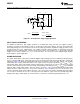
Figure 62 shows a circuit configuration used to measure noise figure for the LMH6553 in a 50Ω system. An R
F
value of 275Ω is chosen for the SO PowerPAD package to minimize output noise while simultaneously allowing
both high gain (9 V/V) and proper 50Ω input termination. Refer to SINGLE-ENDED INPUT TO DIFFERENTIAL
OUTPUT OPERATION for calculation of resistor and gain values. Noise figure values at various frequencies are
shown in Figure 43 in Typical Performance Characteristics.
Figure 62. Noise Figure Circuit Configuration
24 Submit Documentation Feedback Copyright © 2008–2013, Texas Instruments Incorporated
Product Folder Links: LMH6553