
Datasheet


2
V
O
V
G
R
G
R
2
10 k:
LMH6505
3
1
6
7
4
R
F
V
IN
+5V
-5V
R
1
10 k:
R
4
10 k:
R
3
10 k:
0.1 µF
0.1 µF
+5V
-5V
LMH6505
SNOSAT4E –DECEMBER 2005–REVISED APRIL 2013
www.ti.com
The resistors R
S
, R
I
, R
O
, and R
T
are equal to the characteristic impedance, Z
O
, of the transmission line or cable.
Use C
O
to match the output transmission line over a greater frequency range. It compensates for the increase of
the op amp’s output impedance with frequency.
MINIMIZING PARASITIC EFFECTS ON SMALL SIGNAL BANDWIDTH
The best way to minimize parasitic effects is to use surface mount components and to minimize lead lengths and
component distance from the LMH6505. For designs utilizing through-hole components, specifically axial
resistors, resistor self-capacitance should be considered. For example, the average magnitude of parasitic
capacitance of RN55D 1% metal film resistors is about 0.15 pF with variations of as much as 0.1 pF between
lots. Given the LMH6505’s extended bandwidth, these small parasitic reactance variations can cause
measurable frequency response variations in the highest octave. We therefore recommend the use of surface
mount resistors to minimize these parasitic reactance effects.
RECOMMENDATIONS
Here are some recommendations to avoid problems and to get the best performance:
• Do not place a capacitor across R
F
. However, an appropriately chosen series RC combination can be used to
shape the frequency response.
• Keep traces connecting R
F
separated and as short as possible.
• Place a small resistor (20-50Ω) between the output and C
L
.
• Cut away the ground plane, if any, under R
G
.
• Keep decoupling capacitors as close as possible to the LMH6505.
• Connect pin 2 through a minimum resistance of 25Ω.
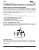
ADJUSTING OFFSETS AND DC LEVEL SHIFTING
Offsets can be broken into two parts: an input-referred term and an output-referred term. These errors can be
trimmed using the circuit in Figure 47. First set V
G
to 0V and adjust the trim pot R
4
to null the offset voltage at the
output. This will eliminate the output stage offsets. Next set V
G
to 2V and adjust the trim pot R
1
to null the offset
voltage at the output. This will eliminate the input stage offsets.
Figure 47. Offset Adjust Circuit
DIGITAL GAIN CONTROL
Digitally variable gain control can be easily realized by driving the LMH6505 gain control input with a digital-to-
analog converter (DAC). Figure 48 illustrates such an application. This circuit employs TI’s eight-bit DAC0830,
the LMC8101 MOS input op amp (Rail-to-Rail Input/Output), and the LMH6505 VGA. With V
REF
set to 2V, the
circuit provides up to 80 dB of gain control in 256 steps with up to 0.05% full scale resolution. The maximum gain
of this circuit is 20 dB.
18 Submit Documentation Feedback Copyright © 2005–2013, Texas Instruments Incorporated
Product Folder Links: LMH6505