
Datasheet


SDI 270 MBPS DATANO DATA
T
2
1485 MBPS DATA 2970 MBPS DATA 270 MBPS DATA
T
1
T
ACQ
T
2
T
2
SDI 270 MBPS DATANO DATA
Lock
Detect
SD/HD
T
2
NO DATA 1485 MBPS DATA NO DATA
T
2
Lock
Detect
SD/HD
T
ACQ
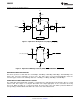
= Acquisition Time, defined in the AC Electrical Characteristics Table
T
1
= Time from Lock Detect assertion or deassertion until SD/HD output is valid, typically 37 ns (one 27 MHz clock period)
T
2
= Time from SDI input change until Lock Detect de-assertion, 1 ms maximum. SD/HD output is not valid during this time.
T
1
T
ACQ
T
1
T
ACQ
T
ACQ
T
1
T
ACQ
T
1
T
1
T
ACQ
T
1
T
1
LMH0356
www.ti.com
SNLS270K –AUGUST 2007–REVISED APRIL 2013
Figure 5. SDI, Lock Detect, and SD/HD Timing
SCO_EN
Input SCO_EN enables the SCO/SDO2 differential output to function either as a serial clock or second serial
data output. SCO/SDO2 functions as a serial clock when SCO_EN is high. This pin has an internal pull-down
device. The default state (low) enables the SCO/SDO2 output as a second serial data output.
ENABLE
The ENABLE pin is used to enable or disable the LMH0356. When the device is disabled, the output drivers and
most of the internal circuitry are powered down. The crystal oscillator / external clock reference circuitry (XTAL IN
and XTAL OUT) remain active regardless of the state of ENABLE, allowing the 27 MHz reference clock signal to
be generated and passed on to additional reclockers. The ENABLE pin is active high and has an internal pull-up
device to enable the LMH0356 by default.
Copyright © 2007–2013, Texas Instruments Incorporated Submit Documentation Feedback 15
Product Folder Links: LMH0356