
Datasheet


LMH0356
www.ti.com
SNLS270K –AUGUST 2007–REVISED APRIL 2013
DEVICE DESCRIPTION
The LMH0356 3 Gbps HD/SD SDI Reclocker with 4:1 Input Mux and FR4 EQs is used in many types of digital
video signal processing equipment. Supported serial digital video standards are SMPTE 259M (C), SMPTE
292M, and SMPTE 424M. Corresponding serial data rates are 270 Mbps, 1.483 Gbps, 1.485 Gbps, 2.967 Gbps,
and 2.97 Gbps. DVB-ASI data at 270 Mbps may also be retimed. The LMH0356 retimes the serial data stream to
suppress accumulated jitter. It provides two low-jitter, differential, serial data outputs. The second output may be
selected to output either serial data or a low-jitter serial data-rate clock. Controls and indicators are: serial clock
or second serial data output select, manual rate select input, SD/HD rate output, lock detect output, auto/manual
data bypass and output mute.
Serial data inputs are CML and LVPECL compatible. Serial data and clock outputs are differential CML and
produce LVPECL compatible levels. The output buffer design can drive AC or DC-coupled, terminated 100Ω
differential loads. The differential output level is 750 mV
P-P
into 100Ω AC or DC-coupled differential loads. Logic
inputs and outputs are LVCMOS compatible.
The device package is a 48-pin WQFN or a 40-pin WQFN. Both package options have an exposed die attach
pad. The exposed die attach pad is electrically connected to device ground (V
EE
) and is the primary electrical
terminal for the device. This terminal must be connected to the negative power supply or circuit ground.
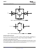
Serial Data Inputs, Serial Data and Clock Outputs
SERIAL DATA INPUT AND OUTPUTS
The differential serial data inputs, SDI0-SDI3, accept serial digital video data at the rates specified in Table 1.
Figure 3 shows the equivalent input circuit for SDI[3:0] and SDI[3:0]. The serial data inputs are differential
LVPECL compatible. These inputs have 50Ω internal terminations (100Ω differential) with an internal bias as
shown in Figure 3. These inputs are intended to be DC coupled to devices such as the LMH0344 adaptive cable
equalizer. DC-coupled inputs must be kept within the specified common mode range. The inputs may be AC
coupled if the input signal is outside the LMH0356's input common mode range (such as when interfacing to 5V
PECL), and in that case the bias is supplied internally so no additional input biasing is required. See Application
Information for more information on input interfacing.
The LMH0356 provides four independent, equalized and multiplexed data inputs. The active input channel is
selected via the SEL0 and SEL1 pins, as shown in Table 2. The equalizer on each of the four inputs is capable
of equalizing up to 30” of FR4 trace without the need for programming for different trace lengths or data rates.
The LMH0356 has two, retimed, differential, serial data outputs, SDO and SCO/SDO2. These outputs provide
low jitter, differential, retimed data to devices such as the LMH0302 cable driver. Output SCO/SDO2 is
multiplexed and can provide either a second serial data output or a serial clock output. Figure 4 shows the
equivalent output circuit for SDO, SDO, SCO/SDO2, and SCO/SDO2.
The SCO_EN input controls the operating mode for the SCO/SDO2 output. When the SCO_EN input is high the
SCO/SDO2 output provides a serial clock. When SCO_EN is low, the SCO/SDO2 output provides retimed serial
data.
Both differential serial data outputs, SDO and SCO/SDO2, are muted when the OUTPUT MUTE input is a logic
low level. SCO/SDO2 also mutes when the Bypass mode is activated when this output is operating as the serial
clock output. When muted, SDO and SDO (or SDO2 and SDO2) will assume opposite differential output levels.
The CML serial data outputs are differential LVPECL compatible. These outputs have internal 50Ω pull-ups and
are suitable for driving AC or DC-coupled, 100Ω center-tapped, AC grounded or 100Ω un-center-tapped,
differentially terminated networks.
Copyright © 2007–2013, Texas Instruments Incorporated Submit Documentation Feedback 11
Product Folder Links: LMH0356