
Datasheet


2
-26
-22
-18
-14
-10
-6
-2
100000
100001000100101
JITTER FREQUENCY (kHz)
JITTER TRANSFER (dB)
-24
-20
-16
-12
-8
-4
0
LMH0040, LMH0050
LMH0070, LMH0340
SNLS271I –APRIL 2007–REVISED APRIL 2013
www.ti.com
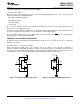
Figure 16. SER Jitter Transfer Function
Register Descriptions
Table 2 provides details on the device's configuration registers.
Table 2. SER Register Detail Table
ADD
Name Bits Field R/W Default Description
'h
00 device_identification The seven MSBs of this register define the SMBus address for the device – the default value is 0x57'h,
but this may be overwritten. The LSB of this register must always be ‘0’ Note that since the address is
shifted over by 1 bit, some systems may address the 57'h as AE'h.
7:1 device id r/w 57'h SMBus device ID
0 Reserved 0'b
01 reset If a ‘1’ is written to bit 0 (LSB) of this register the device will do a soft reset, restoring it’s internal state to
the same as at powerup except device_id register. Once the reset operation is complete, the value in
this register is reset to ‘0’
Bit 4 of this register has a default of 0, if a ‘1’ is written to this location it will disable the analog output
buffer of the device, allowing for some power savings.
7:5 Reserved
4 Analog Dis r/w 0'b Disables Analog
3:1 Reserved
0 sw_rst r/w 0'b software reset
02 GPIO_0 This register configures GPIO_0. Note, if this pin is to be used as an input, then the output must be TRI-
Configuration STATE (bit[0]=’0’) and if used as an output, then the input buffer must be disabled (bit[1]=’0’).
7:4 GPIO_0_mode[3:0] r/w 0000'b 0000: GPout register
0011: TXCLK LOS
0100: TXCLK Detect
0110: Power On Reset
all others: reserved
3:2 GPIO_0_ren[1:0] r/w 01'b 00: pullup and pulldown disabled
01: pulldown enabled
10: pullup enabled
11: Reserved
1 GPIO_0_sleepz r/w 0'b 0: input buffer disabled
1: input buffer enabled
0 GPout0 enable r/w 1'b 0: output TRI-STATE
1: output enabled
20 Submit Documentation Feedback Copyright © 2007–2013, Texas Instruments Incorporated
Product Folder Links: LMH0040 LMH0050 LMH0070 LMH0340