
Datasheet


LMC6572, LMC6574
SNOS707D –DECEMBER 1996–REVISED MARCH 2013
www.ti.com
APPLICATIONS HINTS
LOW VOLTAGE AMPLIFIER TOPOLOGY
The LMC6574/2 incorporates a novel op-amp design topology that enables it to maintain rail-to-rail output swing
even when driving a large load. Instead of relying on a push-pull unity gain output buffer stage, the output stage
is taken directly from the internal integrator, which provides both low output impedance and large gain. Special
feed-forward compensation design techniques are incorporated to maintain stability over a wider range of
operating conditions than traditional micropower op-amps. These features make the LMC6574/2 both easier to
design with, and provide higher speed than products typically found in this ultra-low power class.
COMPENSATING FOR INPUT CAPACITANCE
It is quite common to use large values of feedback resistance for amplifiers with ultra-low input current, like the
LMC6574/2.
Although the LMC6574/2 is highly stable over a wide range of operating conditions, a large feedback resistor will
react even with small values of capacitance at the input of the op-amp to reduce phase margin. The capacitance
at the input of the op-amp comes from transducers, photodiodes and circuit board parasitics.
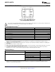
The effect of input capacitance can be compensated for by adding a capacitor, C
f
, around the feedback resistors
(as in Figure 30) such that:
(1)
or
R
1
C
IN
≤ R
2
C
f
(2)
Since it is often difficult to know the exact value of C
IN
, C
f
can be experimentally adjusted so that the desired
pulse response is achieved. Refer to the LMC660 and LMC662 for a more detailed discussion on compensating
for input capacitance.
When high input impedances are demanded, guarding of the LMC6574/2 is suggested. Guarding input lines will
not only reduce leakage, but lowers stray input capacitance as well. (See PRINTED-CIRCUIT-BOARD LAYOUT
FOR HIGH-IMPEDANCE WORK
Figure 30. Cancelling the Effect of Input Capacitance
CAPACITIVE LOAD TOLERANCE
Direct capacitive loading will reduce the phase margin of many op-amps. A pole in the feedback loop is created
by the combination of the op-amp's output impedance and the capacitive load. This pole induces phase lag at the
unity-gain crossover frequency of the amplifier resulting in either an oscillatory or underdamped pulse response.
With a few external components, op amps can easily indirectly drive capacitive loads, as shown in Figure 31.
10 Submit Documentation Feedback Copyright © 1996–2013, Texas Instruments Incorporated
Product Folder Links: LMC6572 LMC6574