
Datasheet


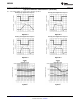


Table Of Contents
- FEATURES
- APPLICATIONS
- DESCRIPTION
- Absolute Maximum Ratings
- Operating Ratings
- DC Electrical Characteristics
- AC Electrical Characteristics
- DC Electrical Characteristics
- AC Electrical Characteristics
- Typical Performance Characteristics
- Application Information
- AMPLIFIER TOPOLOGY
- INPUT COMMON-MODE VOLTAGE RANGE
- RAIL-TO-RAIL OUTPUT
- CAPACITIVE LOAD TOLERANCE
- COMPENSATING FOR INPUT CAPACITANCE
- PRINTED-CIRCUIT-BOARD LAYOUT FOR HIGH-IMPEDANCE WORK
- OFFSET VOLTAGE ADJUSTMENT
- UPGRADING APPLICATIONS
- DATA ACQUISITION SYSTEMS
- INSTRUMENTATION CIRCUITS
- SPICE MACROMODEL
- Typical Single-Supply Applications
- Revision History

LMC6482
SNOS674D –NOVEMBER 1997–REVISED MARCH 2013
www.ti.com
Figure 59. Resistive Isolation of a 330pF Capacitive Load
Figure 60. Pulse Response of the LMC6482 Circuit in Figure 59
Improved frequency response is achieved by indirectly driving capacitive loads, as shown in Figure 61.
Compensated to handle a 330pF capacitive load.
Figure 61. LMC6482 Noninverting Amplifier
R1 and C1 serve to counteract the loss of phase margin by feeding forward the high frequency component of the
output signal back to the amplifiers inverting input, thereby preserving phase margin in the overall feedback loop.
The values of R1 and C1 are experimentally determined for the desired pulse response. The resulting pulse
response can be seen in Figure 62.
18 Submit Documentation Feedback Copyright © 1997–2013, Texas Instruments Incorporated
Product Folder Links: LMC6482