
Datasheet


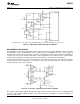

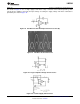

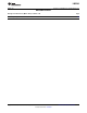


Table Of Contents
- FEATURES
- APPLICATIONS
- DESCRIPTION
- Absolute Maximum Ratings
- Operating Ratings
- DC Electrical Characteristics
- AC Electrical Characteristics
- DC Electrical Characteristics
- AC Electrical Characteristics
- Typical Performance Characteristics
- Application Information
- AMPLIFIER TOPOLOGY
- INPUT COMMON-MODE VOLTAGE RANGE
- RAIL-TO-RAIL OUTPUT
- CAPACITIVE LOAD TOLERANCE
- COMPENSATING FOR INPUT CAPACITANCE
- PRINTED-CIRCUIT-BOARD LAYOUT FOR HIGH-IMPEDANCE WORK
- OFFSET VOLTAGE ADJUSTMENT
- UPGRADING APPLICATIONS
- DATA ACQUISITION SYSTEMS
- INSTRUMENTATION CIRCUITS
- SPICE MACROMODEL
- Typical Single-Supply Applications
- Revision History
LMC6482
www.ti.com
SNOS674D –NOVEMBER 1997–REVISED MARCH 2013
The circuit in Figure 74 uses a single supply to half wave rectify a sinusoid centered about ground. R
I
limits
current into the amplifier caused by the input voltage exceeding the supply voltage. Full wave rectification is
provided by the circuit in Figure 76.
Figure 76. Full Wave Rectifier with Input Current Protection (R
I
)
Figure 77. Full Wave Rectifier Waveform
Figure 78. Large Compliance Range Current Source
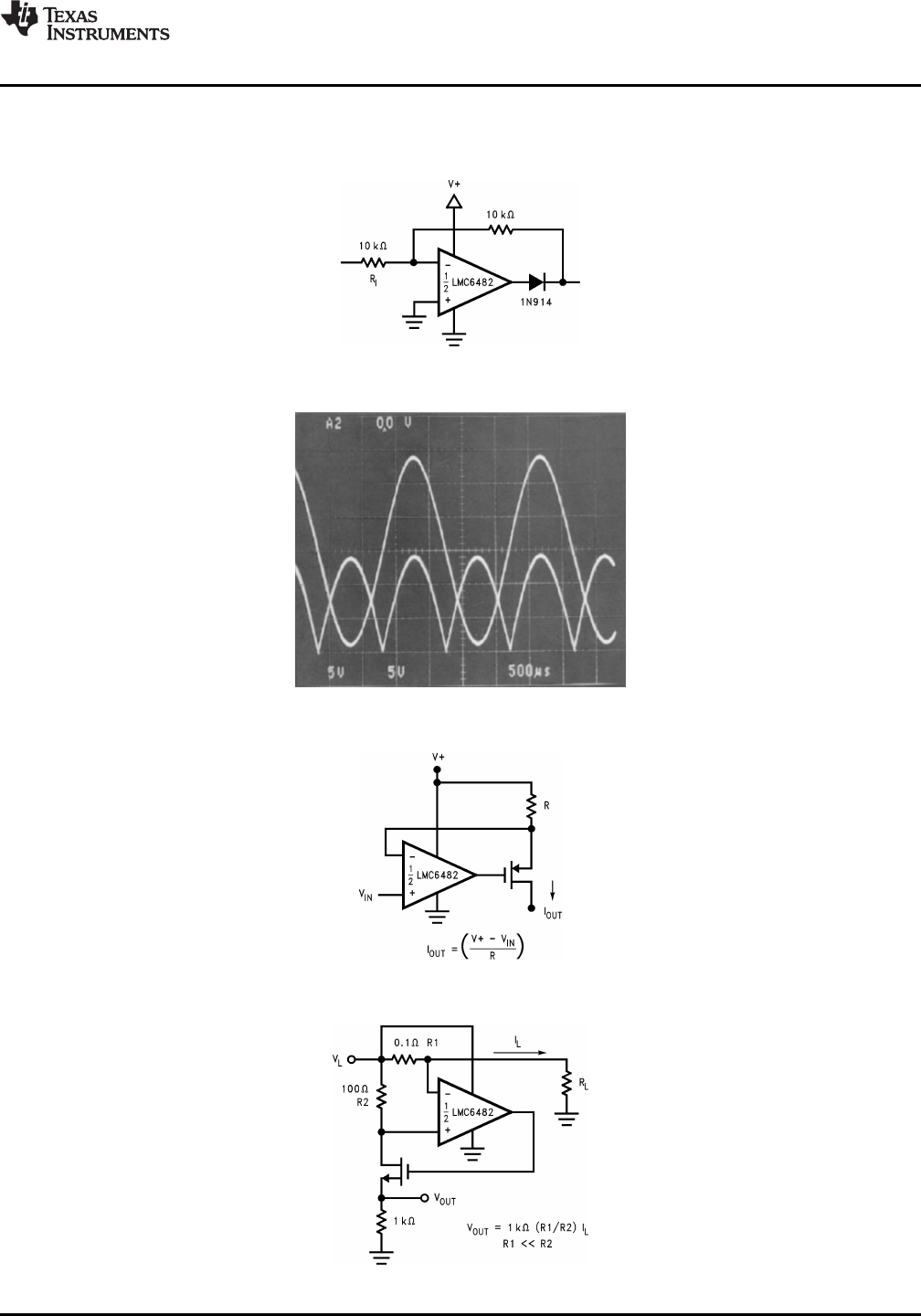
Figure 79. Positive Supply Current Sense
Copyright © 1997–2013, Texas Instruments Incorporated Submit Documentation Feedback 25
Product Folder Links: LMC6482