
Datasheet
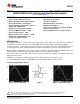


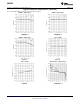
Table Of Contents
- FEATURES
- APPLICATIONS
- DESCRIPTION
- Absolute Maximum Ratings
- Operating Ratings
- DC Electrical Characteristics
- AC Electrical Characteristics
- DC Electrical Characteristics
- AC Electrical Characteristics
- Typical Performance Characteristics
- Application Information
- AMPLIFIER TOPOLOGY
- INPUT COMMON-MODE VOLTAGE RANGE
- RAIL-TO-RAIL OUTPUT
- CAPACITIVE LOAD TOLERANCE
- COMPENSATING FOR INPUT CAPACITANCE
- PRINTED-CIRCUIT-BOARD LAYOUT FOR HIGH-IMPEDANCE WORK
- OFFSET VOLTAGE ADJUSTMENT
- UPGRADING APPLICATIONS
- DATA ACQUISITION SYSTEMS
- INSTRUMENTATION CIRCUITS
- SPICE MACROMODEL
- Typical Single-Supply Applications
- Revision History

LMC6482
www.ti.com
SNOS674D –NOVEMBER 1997–REVISED MARCH 2013
DC Electrical Characteristics
Unless otherwise specified, all limits specified for T
J
= 25°C, V
+
= 5V, V
−
= 0V, V
CM
= V
O
= V
+
/2 and R
L
> 1M. Boldface limits
apply at the temperature extremes.
LMC6482AI LMC6482I LMC6482M
Typ
Parameter Test Conditions Limit Limit Limit Units
(1)
(2) (2) (2)
V
OS
Input Offset Voltage 0.11 0.750 3.0 3.0 mV
1.35 3.7 3.8 max
TCV
OS
Input Offset Voltage
1.0 μV/°C
Average Drift
I
B
Input Current
(3)
0.02 4.0 4.0 10.0 pA
max
I
OS
Input Offset Current
(3)
0.01 2.0 2.0 5.0 pA
max
C
IN
Common-Mode Input
3 pF
Capacitance
R
IN
Input Resistance >10 TeraΩ
CMRR Common Mode Rejection 0V ≤ V
CM
≤ 15.0V 82 70 65 65 dB
Ratio V
+
= 15V min
67 62 60
0V ≤ V
CM
≤ 5.0V 82 70 65 65
V
+
= 5V
67 62 60
+PSRR Positive Power Supply 5V ≤ V
+
≤ 15V, V
−
= 0V 82 70 65 65 dB
Rejection Ratio V
O
= 2.5V
67 62 60 min
−PSRR Negative Power Supply −5V ≤ V
−
≤ −15V, V
+
= 0V 82 70 65 65 dB
Rejection Ratio V
O
= −2.5V
67 62 60 min
V
CM
Input Common-Mode V
+
= 5V and 15V V
−
− 0.3 − 0.25 − 0.25 − 0.25 V
Voltage Range For CMRR ≥ 50dB
0 0 0 max
V
+
+ 0.3V V
+
+ 0.25 V
+
+ 0.25 V
+
+ 0.25 V
V
+
V
+
V
+
min
A
V
Large Signal Voltage Gain R
L
= 2kΩ
(4) (5)
Sourcing 666 140 120 120 V/mV
84 72 60 min
Sinking 75 35 35 35 V/mV
20 20 18 min
R
L
= 600Ω
(4) (5)
Sourcing 300 80 50 50 V/mV
48 30 25 min
Sinking 35 20 15 15 V/mV
13 10 8 min
(1) Typical Values represent the most likely parametric norm.
(2) All limits are specified by testing or statistical analysis.
(3) Ensured limits are dictated by tester limitations and not device performance. Actual performance is reflected in the typical value.
(4) V
+
= 15V, V
CM
= 7.5V and R
L
connected to 7.5V. For Sourcing tests, 7.5V ≤ V
O
≤ 11.5V. For Sinking tests, 3.5V ≤ V
O
≤ 7.5V.
(5) Ensured limits are dictated by tester limitations and not device performance. Actual performance is reflected in the typical value.
Copyright © 1997–2013, Texas Instruments Incorporated Submit Documentation Feedback 3
Product Folder Links: LMC6482