
Datasheet


LMC6032
www.ti.com
SNOS609C –NOVEMBER 1994–REVISED MARCH 2013
CAPACITIVE LOAD TOLERANCE
Like many other op amps, the LMC6032 may oscillate when its applied load appears capacitive. The threshold of
oscillation varies both with load and circuit gain. The configuration most sensitive to oscillation is a unity-gain
follower. See the Typical Performance Characteristics.
The load capacitance interacts with the op amp's output resistance to create an additional pole. If this pole
frequency is sufficiently low, it will degrade the op amp's phase margin so that the amplifier is no longer stable at
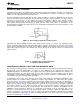
low gains. As shown in Figure 17, the addition of a small resistor (50Ω to 100Ω) in series with the op amp's
output, and a capacitor (5 pF to 10 pF) from inverting input to output pins, returns the phase margin to a safe
value without interfering with lower-frequency circuit operation. Thus, larger values of capacitance can be
tolerated without oscillation. Note that in all cases, the output will ring heavily when the load capacitance is near
the threshold for oscillation.
Figure 17. Rx, Cx Improve Capacitive Load Tolerance
Capacitive load driving capability is enhanced by using a pull up resistor to V
+
(Figure 18). Typically a pull up
resistor conducting 500 μA or more will significantly improve capacitive load responses. The value of the pull up
resistor must be determined based on the current sinking capability of the amplifier with respect to the desired
output swing. Open loop gain of the amplifier can also be affected by the pull up resistor (see DC Electrical
Characteristics).
Figure 18. Compensating for Large Capacitive
Loads with a Pull Up Resistor
PRINTED-CIRCUIT-BOARD LAYOUT FOR HIGH-IMPEDANCE WORK
It is generally recognized that any circuit which must operate with less than 1000 pA of leakage current requires
special layout of the PC board. When one wishes to take advantage of the ultra-low bias current of the
LMC6032, typically less than 0.04 pA, it is essential to have an excellent layout. Fortunately, the techniques for
obtaining low leakages are quite simple. First, the user must not ignore the surface leakage of the PC board,
even though it may sometimes appear acceptably low, because under conditions of high humidity or dust or
contamination, the surface leakage will be appreciable.
To minimize the effect of any surface leakage, lay out a ring of foil completely surrounding the LMC6032's inputs
and the terminals of capacitors, diodes, conductors, resistors, relay terminals, etc. connected to the op-amp's
inputs. See Figure 19. To have a significant effect, guard rings should be placed on both the top and bottom of
the PC board. This PC foil must then be connected to a voltage which is at the same voltage as the amplifier
inputs, since no leakage current can flow between two points at the same potential. For example, a PC board
trace-to-pad resistance of 10
12
Ω, which is normally considered a very large resistance, could leak 5 pA if the
trace were a 5V bus adjacent to the pad of an input. This would cause a 100 times degradation from the
LMC6032's actual performance. However, if a guard ring is held within 5 mV of the inputs, then even a
resistance of 10
11
Ω would cause only 0.05 pA of leakage current, or perhaps a minor (2:1) degradation of the
amplifier's performance. See Figure 20, Figure 21, Figure 22 for typical connections of guard rings for standard
op-amp configurations. If both inputs are active and at high impedance, the guard can be tied to ground and still
provide some protection; see Figure 23.
Copyright © 1994–2013, Texas Instruments Incorporated Submit Documentation Feedback 11
Product Folder Links: LMC6032