
Datasheet


GND
PIN
D1
V+
6.5V
D3
ESD
CLAMP
D2
SNP
GND
D1
PIN
LM95235
LM95235-Q1
SNIS142F –APRIL 2006–REVISED MARCH 2013
www.ti.com
These devices have limited built-in ESD protection. The leads should be shorted together or the device placed in conductive foam
during storage or handling to prevent electrostatic damage to the MOS gates.
Absolute Maximum Ratings
(1)
Supply Voltage, V
DD
-0.3V to 6.0V
Voltage at SMBDAT, SMBCLK, T_CRIT, OS/A0 Pins -0.5V to 6.0V
Voltage at Other Pins (V
DD
+0.3V)
Input Current at D- Pin
(2)
±1 mA
Input Current at All Other Pins
(2)
±5 mA
Output Sink Current, SMBDAT, T_Crit, OS Pins 10 mA
Package Input Current
(2)
30 mA
Human Body Model 2500V
ESD Susceptibility
(3)
Machine Model 250V
Charged Device Model 1000V
Junction Temperature
(4)
+125°C
Storage Temperature -65°C to +150°C
(1) Absolute Maximum Ratings indicate limits beyond which damage to the device may occur. Operating Ratings indicate conditions for
which the device is guaranteed to be functional, but do not guarantee specific performance limits. For guaranteed specifications and test
conditions, see the Electrical Characteristics. The guaranteed specifications apply only for the test conditions listed. Some performance
characteristics may degrade when the device is not operated under the listed test conditions. Operation of the device beyond the
maximum Operating Ratings is not recommended.
(2) When the input voltage (V
I
) at any pin exceeds the power supplies (V
I
< GND or V
I
> V
DD
), the current at that pin should be limited to 5
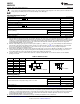
mA. Parasitic components and or ESD protection circuitry are shown in the figures in Table 2 for the LM95235's pins. Care should be
taken not to forward bias the parasitic diodes on pins 2 and 3. Doing so by more than 50 mV may corrupt the temperature
measurements. SNP refers to Snap-back device.
(3) Human body model (HBM) is a charged 100 pF capacitor discharged into a 1.5 kΩ resistor. Machine model (MM), is a charged 200 pF
capacitor discharged directly into each pin. Charged Device Model (CDM) simulates a pin slowly acquiring charge (such as from a
device sliding down the feeder in an automated assembler) then rapidly being discharged.
(4) Thermal resistance junction-to-ambient when attached to a printed circuit board with 1 oz. foil and no airflow is: θ
JA
for VSSOP-8
package = 210°C/W
Table 2. ESD Protection
Pin No. Label Circuit Pin ESD Protection Structure Circuits
1 V
DD
A
2 D+ A
3 D- A
4 T_CRIT B
5 GND A
6 OS/A0 B
Circuit B
7 SMBDAT B
Circuit A
8 SMBCLK B
Operating Ratings
(1)
Operating Temperature Range -40°C to +125°C
LM95235CIMM 0°C ≤ T
A
≤ +90°C
LM95235DIMM -40°C ≤ T
A
≤ +90°C
Electrical Characteristics Temperature Range, T
MIN
≤ T
A
≤ T
MAX
LM95235EIMM -40°C ≤ T
A
≤ +90°C
LM95235QEIMM -40°C ≤ T
A
≤ +85°C
Supply Voltage (V
DD
) +3.0V to +3.6V
Soldering process must comply with Reflow Temperature Profile specifications. Refer to http://www.ti.com/packaging.
(2)
(1) Absolute Maximum Ratings indicate limits beyond which damage to the device may occur. Operating Ratings indicate conditions for
which the device is guaranteed to be functional, but do not guarantee specific performance limits. For guaranteed specifications and test
conditions, see the Electrical Characteristics. The guaranteed specifications apply only for the test conditions listed. Some performance
characteristics may degrade when the device is not operated under the listed test conditions. Operation of the device beyond the
maximum Operating Ratings is not recommended.
(2) Reflow temperature profiles are different for packages containing lead (Pb) than for those that do not.
4 Submit Documentation Feedback Copyright © 2006–2013, Texas Instruments Incorporated
Product Folder Links: LM95235 LM95235-Q1