
Datasheet


LM741
SNOSC25C –MAY 1998–REVISED MARCH 2013
www.ti.com
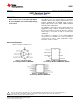
Typical Application
Figure 4. Offset Nulling Circuit
These devices have limited built-in ESD protection. The leads should be shorted together or the device placed in conductive foam
during storage or handling to prevent electrostatic damage to the MOS gates.
Absolute Maximum Ratings
(1)(2)(3)
LM741A LM741 LM741C
Supply Voltage ±22V ±22V ±18V
Power Dissipation
(4)
500 mW 500 mW 500 mW
Differential Input Voltage ±30V ±30V ±30V
Input Voltage
(5)
±15V ±15V ±15V
Output Short Circuit Duration Continuous Continuous Continuous
Operating Temperature Range −55°C to +125°C −55°C to +125°C 0°C to +70°C
Storage Temperature Range −65°C to +150°C −65°C to +150°C −65°C to +150°C
Junction Temperature 150°C 150°C 100°C
Soldering Information
P0008E-Package (10 seconds) 260°C 260°C 260°C
NAB0008A- or LMC0008C-Package (10 seconds) 300°C 300°C 300°C
M-Package
Vapor Phase (60 seconds) 215°C 215°C 215°C
Infrared (15 seconds) 215°C 215°C 215°C
ESD Tolerance
(6)
400V 400V 400V
(1) “Absolute Maximum Ratings” indicate limits beyond which damage to the device may occur. Operating Ratings indicate conditions for
which the device is functional, but do not ensure specific performance limits.
(2) For military specifications see RETS741X for LM741 and RETS741AX for LM741A.
(3) If Military/Aerospace specified devices are required, please contact the TI Sales Office/Distributors for availability and specifications.
(4) For operation at elevated temperatures, these devices must be derated based on thermal resistance, and T
j
max. (listed under “Absolute
Maximum Ratings”). T
j
= T
A
+ (θ
jA
P
D
).
(5) For supply voltages less than ±15V, the absolute maximum input voltage is equal to the supply voltage.
(6) Human body model, 1.5 kΩ in series with 100 pF.
Electrical Characteristics
(1)
LM741A LM741 LM741C
Parameter Test Conditions Units
Min Typ Max Min Typ Max Min Typ Max
Input Offset Voltage T
A
= 25°C
R
S
≤ 10 kΩ 1.0 5.0 2.0 6.0 mV
R
S
≤ 50Ω 0.8 3.0
T
AMIN
≤ T
A
≤ T
AMAX
R
S
≤ 50Ω 4.0 mV
R
S
≤ 10 kΩ 6.0 7.5
Average Input Offset Voltage
15 μV/°C
Drift
(1) Unless otherwise specified, these specifications apply for V
S
= ±15V, −55°C ≤ T
A
≤ +125°C (LM741/LM741A). For the LM741C/LM741E,
these specifications are limited to 0°C ≤ T
A
≤ +70°C.
2 Submit Documentation Feedback Copyright © 1998–2013, Texas Instruments Incorporated
Product Folder Links: LM741