
Datasheet


Snap
Back
GND
D1
PIN
Snap
Back
GND
D1
PIN
V
DD
125
D2
D3
Snap
Back
GND
D1
PIN
Snap
Back
GND
D1
PIN
V
DD
2.5k
D2
D3
ADDR
SMBCLK
LM73
1
2
3
4
5
GND
SMBDAT
V
DD
6
ALERT
LM73
www.ti.com
SNIS141D –OCTOBER 2005–REVISED MAY 2009
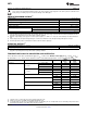
Connection Diagram
Figure 1. SOT-6 (TOP VIEW)
PIN DESCRIPTIONS
Label Pin # Type Equivalent Circuit Function
ADDR 1 CMOS Logic Address Select Input: One of three device
Input addresses is selected by connecting to ground,
(three levels) left floating, or connecting to V
DD
.
GND 2 Ground Ground
V
DD
3 Power Supply Voltage
SMBCLK 4 CMOS Logic Serial Clock: SMBus clock signal. Operates up
Input to 400 kHz. Low-pass filtered.
ALERT 5 Open-Drain Digital output which goes active whenever the
Output measured temperature exceeds a
programmable temperature limit.
SMBDAT 6 Open-Drain Serial Data: SMBus bi-directional data signal
Input/Output used to transfer serial data synchronous to the
SMBCLK. Low-pass filtered.
Copyright © 2005–2009, Texas Instruments Incorporated Submit Documentation Feedback 3
Product Folder Links: LM73