
Datasheet


LM6511
SNOS695C –JUNE 1999–REVISED MARCH 2013
www.ti.com
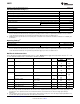
Absolute Maximum Ratings
(1)(2)
Supply Voltage −0.3 to +36V
Output to Negative Supply Voltage 50V
Ground to Negative Supply Voltage 30V
Differential Input Voltage ±30V
Input Voltage See
(1)
Storage Temperature Range −65°C to +150°C
Soldering Information: SOIC Package (Vapor Phase in 60 sec) 215°C
SOIC Package (Infrared in 15 sec) 220°C
Power Dissipation 500 mW
Output Short Circuit Duration 10s
Junction Temperature 150°C
ESD Rating (C = +100 pF, R = 1.5 kΩ) 300V
(1) Absolute Maximum Ratings indicate limits beyond which damage to the device may occur. Operating ratings indicate conditions the
device is intended to be functional, but do not guarantee specific performance limits. For guaranteed specifications and test conditions,
see the Electrical Characteristics. The guaranteed specifications apply only for the test conditions listed.
(2) If Military/Aerospace specified devices are required, please contact the Texas Instruments Sales Office/ Distributors for availability and
specifications.
Operating Ratings
(1)
Supply Voltage 2.5V to 30V
Temperature Range −40°C ≤ T
J
≤ +85°C
Thermal Resistance (θ
JA
) SOIC Package 170°C/W
(1) Absolute Maximum Ratings indicate limits beyond which damage to the device may occur. Operating ratings indicate conditions the
device is intended to be functional, but do not guarantee specific performance limits. For guaranteed specifications and test conditions,
see the Electrical Characteristics. The guaranteed specifications apply only for the test conditions listed.
DC Electrical Characteristics
Unless otherwise specified, all limits guaranteed for T
J
= 25°C. Boldface limits apply at the temperature extremes. V
+
= 2.7V,
V
−
= 0V, 50Ω ≤ R
L
≤ 50kΩ, and I
L
= 1.0 mA unless otherwise specified
Symbol Parameter Conditions Typical LM6511I Units
(Limits)
Limit
V
OS
Offset Voltage R
S
≤ 50 kΩ
(1)
1.5 5 mV
8 max
I
B
Input Bias Current 38 130 nA
max
200
I
OS
Input Offset Current R
S
≤ 50 kΩ
(1)
1.5 20 nA
max
50
I
S
Positive Supply Current 2.7 3.5
5
mA
max
Negative Supply Current 1.5 2.0
2.5
V
SAT
Saturation Voltage V
IN
≤ 10 mV 0.23 0.4 V
I
SINK
= 8 mA
0.4 max
A
V
Large Signal Voltage Gain ΔV
OUT
= 2V 40 V/mV
CMRR Common Mode Rejection Ratio 72 dB
I
STROBE
Strobe ON Current See
(2)
2.0 5.0 mA
max
(1) The offset voltage and offset current limits are the maximum values required to drive the output within a volt of either supply with a 1 mA
load. Therefore, these parameters define an error band and take into account the worst-case effects of voltage gain and input
impedance.
(2) This specification gives the range of current which must be drawn from the strobe pin to ensure the output is properly disabled. Do not
short the strobe pin to ground; it should be current driven at 3 mA to 5 mA.
2 Submit Documentation Feedback Copyright © 1999–2013, Texas Instruments Incorporated
Product Folder Links: LM6511