
Datasheet


LM5642, LM5642X
SNVS219K –JUNE 2003–REVISED APRIL 2013
www.ti.com
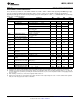
ELECTRICAL CHARACTERISTICS (continued)
Unless otherwise specified, V
IN
= 28V, GND = PGND = 0V, VLIN5 = VDD1 = VDD2. Limits appearing in boldface type apply
over the specified operating junction temperature range, (-40°C to +125°C, if not otherwise specified). Specifications
appearing in plain type are measured using low duty cycle pulse testing with T
A
= 25°C
(1)
,
(2)
. Min/Max limits are specified by
design, test, or statistical analysis.
Symbol Parameter Conditions Min Typ Max Units
Gate Drive
I
CBOOT
CBOOTx Leakage Current V
CBOOT1
= V
CBOOT2
= 7V 10 nA
I
SC_DRV
HDRVx and LDRVx Source V
CBOOT1
= V
CBOOT2
= 5V, VSWx=0V,
0.5 A
Current HDRVx=LDRVx=2.5V
I
sk_HDRV
HDRVx Sink Current V
CBOOTx
= VDDx = 5V, V
SWx
= 0V, HDRVX
0.8 A
= 2.5V
I
sk_LDRV
LDRVx Sink Current V
CBOOTx
= VDDx = 5V, V
SWx
= 0V, LDRVX
1.1 A
= 2.5V
R
HDRV
HDRV1 & 2 Source On- V
CBOOT1
= V
CBOOT2
= 5V,
3.1 Ω
Resistance V
SW1
= V
SW2
= 0V
HDRV1 & 2 Sink On-
1.5 Ω
Resistance
R
LDRV
LDRV1 & 2 Source On- V
CBOOT1
= V
CBOOT2
= 5V,
3.1 Ω
Resistance V
SW1
= V
SW2
= 0V
V
DD1
= V
DD1
= 5V
LDRV1 & 2 Sink On-
1.1 Ω
Resistance
Oscillator and Sync Controls
5.5 ≤ V
IN
≤ 36V, LM5642 166 200 226
F
osc
Oscillator Frequency kHz
5.5 ≤ V
IN
≤ 36V, LM5642X 311 375 424
Don_max Maximum On-Duty Cycle V
FB1
= V
FB2
= 1V, Measured at pins
96 98.9 %
HDRV1 and HDRV2
T
on_min
Minimum On-Time 166 ns
SS
OT_delta
HDRV1 and HDRV2 Delta ON/SS1 = ON/SS2 = 2V
20 250 ns
On Time
V
HS
SYNC Pin Min High Input 2 1.52 V
V
LS
SYNC Pin Max Low Input 1.44 0.8 V
Error Amplifier
I
FB1
, I
FB2
Feedback Input Bias V
FB1_FIX
= 1.5V, V
FB2_FIX
= 1.5V
80 ±200 nA
Current
I
comp1_SC
, COMP Output Source V
FB1_FIX
= V
FB2_FIX
= 1V,
6 127
I
comp2_SC
Current V
COMP1
= V
COMP2
= 1V
µA
-20°C to 85°C 18
I
comp1_SK
, COMP Output Sink Current V
FB1_FIX
= V
FB2_FIX
= 1.5V and
6 118
I
comp2_SK
V
COMP1
= V
COMP2
= 0.5V
µA
-20°C to 85°C 18
gm1, gm2 Transconductance 720 µmho
GI
SNS1
, Current Sense Amplifier V
COMPx
= 1.25V
4.2 5.2 7.5
GI
SNS2
(1&2) Gain
Voltage References and Linear Voltage Regulators
UVLO VLIN5 Under-voltage ON/SS1, ON/SS2 transition
Lockout from low to high 3.6 4.0 4.4 V
Threshold Rising
6 Submit Documentation Feedback Copyright © 2003–2013, Texas Instruments Incorporated
Product Folder Links: LM5642 LM5642X