
Datasheet


LM5642, LM5642X
www.ti.com
SNVS219K –JUNE 2003–REVISED APRIL 2013
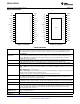
PIN DESCRIPTIONS (continued)
Compensation pin for Channel 2. This is the output of the internal transconductance error amplifier. The loop
COMP2 (Pin 12)
compensation network should be connected between this pin and the signal ground SGND (Pin 8).
Current limit threshold setting for Channel 2. See ILIM1 (Pin 2).
ILIM2 (Pin 13)
The positive (+) Kelvin sense for the internal current sense amplifier of Channel 2. See KS1 (Pin 1).
KS2 (Pin 14)
The negative (-) Kelvin sense for the internal current sense amplifier of Channel 2. Connect this pin to the low side
RSNS2 (Pin 15)
of the current sense resistor that is placed between VIN and the drain of the top MOSFET. When the Rds of the
top MOSFET is used for current sensing, connect this pin to the source of the top MOSFET. Always use a
separate trace to form a Kelvin connection to this pin.
Switch-node connection for Channel 2, which is connected to the source of the top MOSFET of Channel 2. It
SW2 (Pin 16)
serves as the negative supply rail for the top-side gate driver, HDRV2.
Top-side gate-drive output for Channel 2. HDRV is a floating drive output that rides on the corresponding
HDRV2 (Pin 17)
switching-node voltage.
Bootstrap capacitor connection. It serves as the positive supply rail for the Channel 2 top-side gate drive. Connect
CBOOT2 (Pin 18)
this pin to VDD2 (Pin 19) through a diode, and connect the low side of the bootstrap capacitor to SW2 (Pin16).
The supply rail for the Channel 2 low-side gate drive. Connected to VLIN5 (Pin 7) through a 4.7Ω resistor and
VDD2 (Pin 19)
bypassed to power ground with a ceramic capacitor of at least 1µF. Tie this pin to VDD1 (Pin 24).
Low-side gate-drive output for Channel 2.
LDRV2 (Pin 20)
The power ground connection for both channels. Connect to the ground rail of the system.
PGND (Pin 21)
The power input pin for the chip. Connect to the positive (+) input rail of the system. This pin must be connected
VIN (Pin 22)
to the same voltage rail as the top FET drain (or the current sense resistor when used).
Low-side gate-drive output for Channel 1.
LDRV1 (Pin 23)
The supply rail for Channel 1 low-side gate drive. Tie this pin to VDD2 (Pin 19).
VDD1 (Pin 24)
Bootstrap capacitor connection. This pin serves as the positive supply rail for the Channel 1 top-side gate drive.
CBOOT1 (Pin 25)
See CBOOT2 (Pin 18).
Top-side gate-drive output for Channel 1. See HDRV2 (Pin 17).
HDRV1 (Pin 26)
Switch-node connection for Channel 1. See SW2 (Pin16).
SW1 (Pin 27)
The negative (-) Kelvin sense for the internal current sense amplifier of Channel 1. See RSNS2 (Pin 15).
RSNS1 (Pin 28)
The power ground connection for both channels. Connect to the ground rail of the system. Use of multiple vias to
PGND (DAP)
internal ground plane or GND layer helps to dissipate heat generated by output power.
Copyright © 2003–2013, Texas Instruments Incorporated Submit Documentation Feedback 3
Product Folder Links: LM5642 LM5642X