
Datasheet


RAMP
( )
( )
ON
IN OUT
RAMP
t
5 V V 25
C
m ´ - - m ´
t
ON
Sample and Hold DC Level
0.5V/A
LM5576, LM5576-Q1
www.ti.com
SNVS447I –JANUARY 2007–REVISED APRIL 2013
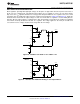
Error Amplifier and PWM Comparator
The internal high gain error amplifier generates an error signal proportional to the difference between the
regulated output voltage and an internal precision reference (1.225V). The output of the error amplifier is
connected to the COMP pin allowing the user to provide loop compensation components, generally a type II
network, as illustrated in Figure 9. This network creates a pole at DC, a zero and a noise reducing high
frequency pole. The PWM comparator compares the emulated current sense signal from the RAMP generator to
the error amplifier output voltage at the COMP pin.
RAMP Generator
The ramp signal used in the pulse width modulator for current mode control is typically derived directly from the
buck switch current. This switch current corresponds to the positive slope portion of the output inductor current.
Using this signal for the PWM ramp simplifies the control loop transfer function to a single pole response and
provides inherent input voltage feed-forward compensation. The disadvantage of using the buck switch current
signal for PWM control is the large leading edge spike due to circuit parasitics that must be filtered or blanked.
Also, the current measurement may introduce significant propagation delays. The filtering, blanking time and
propagation delay limit the minimum achievable pulsewidth. In applications where the input voltage may be
relatively large in comparison to the output voltage, controlling small pulsewidths and duty cycles is necessary for
regulation. The LM5576 utilizes a unique ramp generator, which does not actually measure the buck switch
current but rather reconstructs the signal. Reconstructing or emulating the inductor current provides a ramp
signal to the PWM comparator that is free of leading edge spikes and measurement or filtering delays. The
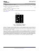
current reconstruction is comprised of two elements; a sample & hold DC level and an emulated current ramp.
Figure 14. Composition of Current Sense Signal
The sample & hold DC level illustrated in Figure 14 is derived from a measurement of the re-circulating Schottky
diode anode current. The re-circulating diode anode should be connected to the IS pin. The diode current flows
through an internal current sense resistor between the IS and PGND pins. The voltage level across the sense
resistor is sampled and held just prior to the onset of the next conduction interval of the buck switch. The diode
current sensing and sample & hold provide the DC level of the reconstructed current signal. The positive slope
inductor current ramp is emulated by an external capacitor connected from the RAMP pin to AGND and an
internal voltage controlled current source. The ramp current source that emulates the inductor current is a
function of the Vin and Vout voltages per the following equation:
I
RAMP
= (5µ x (Vin – Vout)) + 25µA (2)
Copyright © 2007–2013, Texas Instruments Incorporated Submit Documentation Feedback 11
Product Folder Links: LM5576 LM5576-Q1