
Datasheet


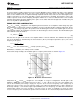


V
IN
V
OUT1
V
OUT2
C
OUT1
C
OUT2
C
IN1
C
IN2
PGND2
PGND1
AGND
R
FB2A
R
FB1A
R
FB1B
R
FB2B
The bold lines indicate a solid ground plane. Make the
traces to the widest and the shortest and use the star
ground technique.
These lines indicate the high current paths. Make the
traces as wide and short as possible
These lines indicate the small signal paths. The traces
can be narrow but keep them away from any radiated
noise and away from traces that may couple noise
capacitively
These points require the maximum bypassing of the high
frequency switching noise. Isolate each channel from the
high frequency switching noise of the other channel.
Loop1
Loop2
CS1 CS2
CSG1 CSG2
EP
LM5119/LM5119Q
SNVS676F –AUGUST 2010–REVISED FEBRUARY 2013
www.ti.com
Figure 16. Recommended PCB Layout
28 Submit Documentation Feedback Copyright © 2010–2013, Texas Instruments Incorporated
Product Folder Links: LM5119/LM5119Q