
Datasheet


LM5119/LM5119Q
SNVS676F –AUGUST 2010–REVISED FEBRUARY 2013
www.ti.com
To configure the LM5119 for interleaved operation, connect COMP1 and COMP2 pins together at the IC.
Connecting the FB2 pin to VCC2 pin will disable the channel2 error amplifier with a high output impedance at
COMP2. Connect the compensation network between FB1 and the common COMP pins. Connect the two power
stages together at the output capacitors. Finally use the plots in Figure 13 and Figure 14 along with the duty
cycle range to determine the amount of output and input capacitor ripple reduction. Frequently more capacitance
than necessary is used in a design just to meet ESR requirements. Reducing the capacitance based solely on
ripple reduction graphs alone may violate this requirement.
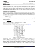
In the LM5119 evaluation board (schematic shown in Figure 15) interleaved operation can be enabled by
shorting both outputs together (with identical components in the power train), and using zero ohm resistors for
R22 and R21. This shorts VCC2 to FB2 and COMP2 to COMP1 respectively. Also the channel2 feedback
network C14, R6, and C15 should be removed. The easy re-configuration between two channel and single
channel operation will allow insight into the benefits of interleaved operation.
Figure 15. 10V 4A, 5V 8A Typical Application Schematic
26 Submit Documentation Feedback Copyright © 2010–2013, Texas Instruments Incorporated
Product Folder Links: LM5119/LM5119Q