
Datasheet


LM5119/LM5119Q
SNVS676F –AUGUST 2010–REVISED FEBRUARY 2013
www.ti.com
/ (2π x R
COMP
x C
COMP
) to be about 1.1kHz. Increasing R
COMP
, while proportionally decreasing C
COMP
, increases
the error amp gain. Conversely, decreasing R
COMP
while proportionally increasing C
COMP
, decreases the error
amp gain. For the design example C
COMP
was selected as 6800pF and R
COMP
was selected as 36.5kΩ. These
values configure the compensation network zero at 640Hz. The error amp gain at frequencies greater than f
ZEA
is: R
COMP
/ R
FB2
, which is approximately 5.22 (14.3dB).
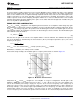
Figure 11. Error Amplifier Gain and Phase
The overall voltage loop gain can be predicted as the sum (in dB) of the modulator gain and the error amp gain.
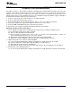
Figure 12. Overall Voltage Loop Gain and Phase
If a network analyzer is available, the modulator gain can be measured and the error amplifier gain can be
configured for the desired loop transfer function. If the K factor is between 2 and 3, the stability should be
checked with the network analyzer. If a network analyzer is not available, the error amplifier compensation
components can be designed with the guidelines given. Step load transient tests can be performed to verify
acceptable performance. The step load goal is minimum overshoot with a damped response. C
HF
can be added
to the compensation network to decrease noise susceptibility of the error amplifier. The value of C
HF
must be
sufficiently small since the addition of this capacitor adds a pole in the error amplifier transfer function. This pole
must be well beyond the loop crossover frequency. A good approximation of the location of the pole added by
C
HF
is: f
P2
= f
ZEA
x C
COMP
/ C
HF
. The value of C
HF
was selected as 100pF for the design example.
MISCELLANEOUS FUNCTIONS
EN2 is left floating which allows channel2 to always remain enabled. If EN2 is pulled below 2V, channel2 is
disabled.
The DEMB pin is left floating since this design uses diode emulation. For fully synchronous (continuous
conduction) operation, connect the DEMB to a voltage greater than 2.6V.
VCCDIS is left floating to enable the internal VCC regulators. To disable the internal VCC regulators, connect this
pin to a voltage greater than 1.25V.
24 Submit Documentation Feedback Copyright © 2010–2013, Texas Instruments Incorporated
Product Folder Links: LM5119/LM5119Q