
Datasheet


HB
VOUT
CSG
CS
LO
HO
HS
LM5118
VIN
D1
Q2 (OFF)
D2
Q1
Buck Switch
Current
Diode Current
LM5118, LM5118-Q1
www.ti.com
SNVS566G –APRIL 2008–REVISED FEBRUARY 2013
DETAILED OPERATING DESCRIPTION
The LM5118 high voltage switching regulator features all of the functions necessary to implement an efficient
high voltage buck or buck-boost regulator using a minimum of external components. The regulator switches
smoothly from buck to buck-boost operation as the input voltage approaches the output voltage, allowing
operation with the input greater than or less than the output voltage. This easy to use regulator integrates high-
side and low-side MOSFET drivers capable of supplying peak currents of 2 Amps. The regulator control method
is based on current mode control utilizing an emulated current ramp. Peak current mode control provides
inherent line feed-forward, cycle-by-cycle current limiting and ease of loop compensation. The use of an
emulated control ramp reduces noise sensitivity of the pulse-width modulation circuit, allowing reliable processing
of very small duty cycles necessary in high input voltage applications. The operating frequency is user
programmable from 50 kHz to 500 kHz. An oscillator synchronization pin allows multiple LM5118 regulators to
self synchronize or be synchronized to an external clock. Fault protection features include current limiting,
thermal shutdown and remote shutdown capability. An under-voltage lockout input allows regulator shutdown
when the input voltage is below a user selected threshold, and a low state at the enable pin will put the regulator
into an extremely low current shutdown state. The device is available in the HTSSOP-20EP package featuring an
exposed pad to aid in thermal dissipation.
A buck-boost regulator can maintain regulation for input voltages either higher or lower than the output voltage.
The challenge is that buck-boost power converters are not as efficient as buck regulators. The LM5118 has been
designed as a dual mode controller whereby the power converter acts as a buck regulator while the input voltage
is above the output. As the input voltage approaches the output voltage, a gradual transition to the buck-boost
mode occurs. The dual mode approach maintains regulation over a wide range of input voltages, while
maintaining the optimal conversion efficiency in the normal buck mode. The gradual transition between modes
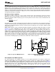
eliminates disturbances at the output during transitions. Figure 10 shows the basic operation of the LM5118
regulator in the buck mode. In buck mode, transistor Q1 is active and Q2 is disabled. The inductor current ramps
in proportion to the VIN - VOUT voltage difference when Q1 is active and ramps down through the recirculating
diode D1 when Q1 is off. The first order buck mode transfer function is VOUT/VIN = D, where D is the duty cycle
of the buck switch, Q1.
Figure 10. Buck Mode Operation
Figure 11 shows the basic operation of buck-boost mode. In buck-boost mode both Q1 and Q2 are active for the
same time interval each cycle. The inductor current ramps up (proportional to VIN) when Q1 and Q2 are active
and ramps down through the recirculating diode during the off time. The first order buck-boost transfer function is
VOUT/VIN = D/(1-D), where D is the duty cycle of Q1 and Q2.
Copyright © 2008–2013, Texas Instruments Incorporated Submit Documentation Feedback 11
Product Folder Links: LM5118 LM5118-Q1