
Datasheet

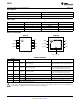


1
2
3
5
6
4
VDD
VSS
IN
INB
Exposed Pad
SOT-23
1
2
3
5
6
4
VDD
P_OUT
N_OUT VSS
IN
INB
P_OUT
N_OUT
WQFN-6
LM5114
SNVS790E –JANUARY 2012–REVISED MARCH 2013
www.ti.com
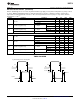
Input Options
Base Part Number Input Thresholds
LM5114A CMOS
LM5114B TTL
Truth Table
IN INB P_OUT N_OUT
L L OPEN L
L H OPEN L
H L H OPEN
H H OPEN L
Connection Diagram
PIN DESCRIPTIONS
Pin No.
Name Description Applications Information
SOT-23-6 WQFN-6
Locally decouple to VSS using low ESR/ESL
1 1 VDD Gate drive supply capacitor located as close as possible to the
IC.
Connect to the gate of the MOSFET with a
2 2 P_OUT Source-current output short, low inductance path. A gate resistor
can be used to adjust the turn-on speed.
Connect to the gate of the MOSFET with a
3 3 N_OUT Sink-current output short, low inductance path. A gate resistor
can be used to adjust the turn-off speed.
4 4 VSS Ground All signals are referenced to this ground.
5 5 INB Inverting logic input Connect to VSS when not used.
6 6 IN Non-inverting logic input Connect to VDD when not used.
It is recommended that the exposed pad on the bottom of the package is soldered to ground plane on the PC
EP
board to aid thermal dissipation.
These devices have limited built-in ESD protection. The leads should be shorted together or the device placed in conductive foam
during storage or handling to prevent electrostatic damage to the MOS gates.
2 Submit Documentation Feedback Copyright © 2012–2013, Texas Instruments Incorporated
Product Folder Links: LM5114