
Datasheet


7V to 55V
Input
V
IN
GND
SHUTDOWN
C
IN
33 PF
C
BYP
1 PF
R
T
90.9 k:
GND
FB
PGATE
ISEN
ADJ
VCC
C
VCC
0.47 PF
C
ADJ
1000 pF
R
ADJ
2.1 k:
R
SEN
0.01:
L1 15 PH
Q1
D1
V
OUT
C
OUT
GND
C1
3300 pF
C2
0.1 PF
R3
66.5 k:
5V
100 PF
R
FB1
3.4 k:
R
FB2
10 k:
RT
VIN
LM5085
LM5085, LM5085-Q1
SNVS565G –NOVEMBER 2008–REVISED MARCH 2013
www.ti.com
P
DISS
= 55V x ((40nC x 300kHz) + 1.4mA) = 737mW (32)
Using an HVSSOP package with a θ
JA
of 46°C/W produces a temperature rise of 34°C from junction to ambient.
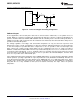
Final Design Example Circuit
The final circuit is shown in Figure 28, and its performance is presented in Figure 29 through Figure 32.
Figure 28. Example Circuit
Figure 29. Efficiency vs. Load Current and V
IN
Figure 30. Frequency vs. V
IN
(Circuit of Figure 28) (Circuit of Figure 28)
Figure 31. Current Limit vs. V
IN
Figure 32. LM5085 Power Dissipation
(Circuit of Figure 28) (Circuit of Figure 28)
18 Submit Documentation Feedback Copyright © 2008–2013, Texas Instruments Incorporated
Product Folder Links: LM5085 LM5085-Q1